SLLSEV4 February 2017 TUSB319-Q1
PRODUCTION DATA.
- 1 Features
- 2 Applications
- 3 Description
- 4 Revision History
- 5 Pin Configuration and Functions
- 6 Specifications
- 7 Detailed Description
- 8 Application and Implementation
- 9 Power Supply Recommendations
- 10Layout
- 11Device and Documentation Support
- 12Mechanical, Packaging, and Orderable Information
8 Application and Implementation
NOTE
Information in the following applications sections is not part of the TI component specification, and TI does not warrant its accuracy or completeness. TI’s customers are responsible for determining suitability of components for their purposes. Customers should validate and test their design implementation to confirm system functionality.
8.1 Application Information
The TUSB319-Q1 device is a Type-C configuration channel logic and port controller. The TUSB319-Q1 device can detect when a Type-C device is attached, what type of device is attached, the orientation of the cable, and power capabilities, this power capabilities are sourcing only since the TUSB319-Q1 device can be used in a source application (DFP) only.
8.2 Typical Application
8.2.1 DFP Mode
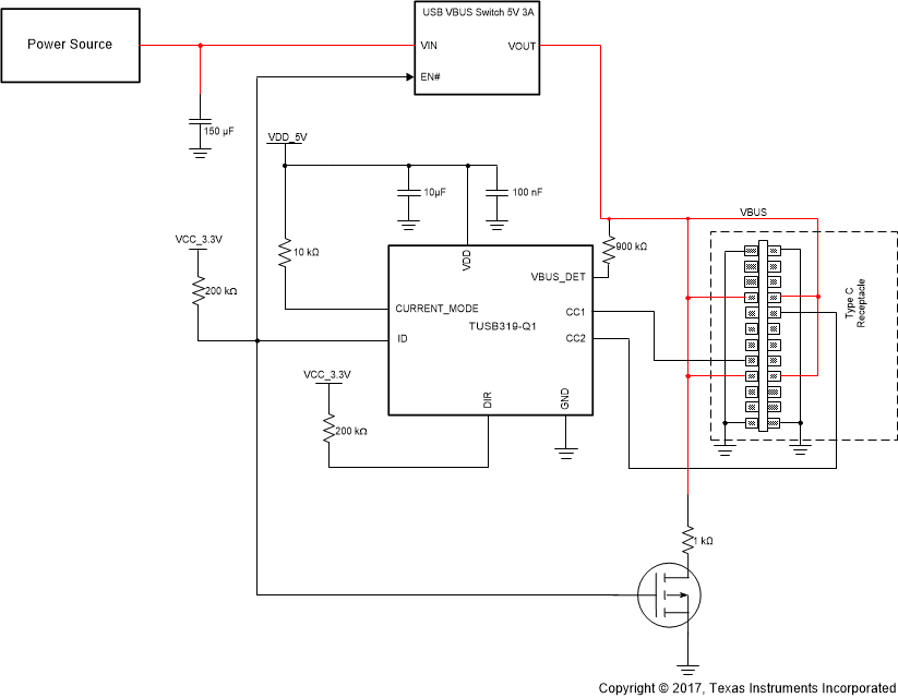
Figure 2 shows the TUSB319-Q1 on a DFP port with USB3 functionality.
 Figure 2. DFP Mode Schematic
8.2.1.1 Design Requirements
For this design example, use the parameters listed in Table 4:
Table 4. Design Requirements for DFP Mode
| DESIGN PARAMETER | VALUE |
|---|---|
| VDD (3.8 V to 5.5 V) | 5 V |
| Advertised Type-C Current (Default, 1.5 A, 3 A) | 3 A |
8.2.1.2 Detailed Design Procedure
The TUSB319-Q1 device supports a VDD in the range of 3.8 V to 5.5 V. In this particular case, VDD is set to 5 V. A 100-nF capacitor is placed near VDD.
The TUSB319-Q1 current advertisement is determined by the state of the CURRENT_MODE pin. In this particular example, 3 A advertisement is desired so the CURRENT_MODE pin is pulled high to VDD through 10-kΩ resistor.
The VBUS_DET pin must be connected through a 900-kΩ resistor to VBUS on the Type-C that is connected. This large resistor is required to protect the TUSB319-Q1 device from large VBUS voltage that is possible in present day systems. This resistor along with internal pulldown keeps the voltage observed by the TUSB319-Q1 device in the recommended range.
The USB2 specification requires the bulk capacitance on VBUS of at least 120 µF. In this particular case, a 150-µF capacitor was chosen.
TUSB319-Q1 does not provide VBUS discharge and requires an external solution either through switched resistor pull-down as shown in Figure 2 or elsewhere in the system.
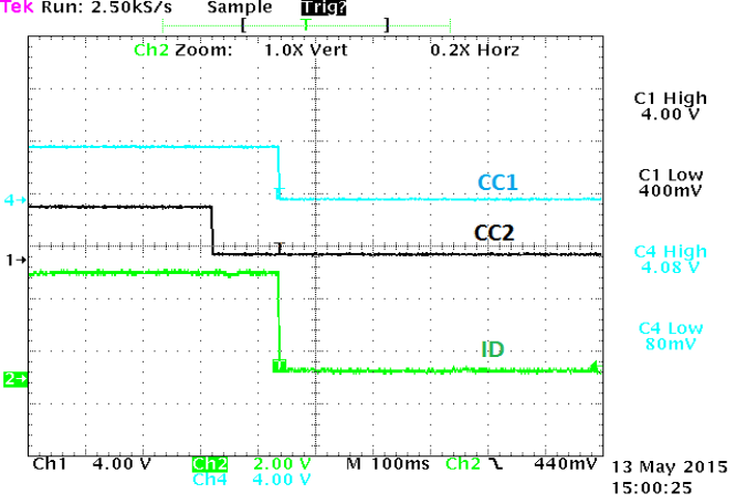
8.2.1.3 Application Curve
 Figure 3. CC Detection
8.3 Initialization Set Up
The general power-up sequence for the TUSB319-Q1 device is as follows:
- System is powered off (device has no VDD).
- VDD ramps – POR circuit.
- The TUSB319-Q1 device enters unattached mode.
- The TUSB319-Q1 device monitors the CC pins.
- The TUSB319-Q1 device enters active mode when attach has been successfully detected.