SLLSEV4 February 2017 TUSB319-Q1
PRODUCTION DATA.
- 1 Features
- 2 Applications
- 3 Description
- 4 Revision History
- 5 Pin Configuration and Functions
- 6 Specifications
- 7 Detailed Description
- 8 Application and Implementation
- 9 Power Supply Recommendations
- 10Layout
- 11Device and Documentation Support
- 12Mechanical, Packaging, and Orderable Information
6 Specifications
6.1 Absolute Maximum Ratings
over operating free-air temperature range (unless otherwise noted)(1)| MIN | MAX | UNIT | ||
|---|---|---|---|---|
| Supply voltage | VDD | –0.3 | 6 | V |
| Control pins | CC1, CC2, CURRENT_MODE, ID, DIR | –0.3 | 6 | V |
| VBUS_DET | –0.3 | 4 | ||
| Storage temperature, Tstg | –65 | 150 | °C | |
(1) Stresses beyond those listed under Absolute Maximum Ratings may cause permanent damage to the device. These are stress ratings only, which do not imply functional operation of the device at these or any other conditions beyond those indicated under Recommended Operating Conditions. Exposure to absolute-maximum-rated conditions for extended periods may affect device reliability.
6.2 ESD Ratings
| VALUE | UNIT | |||
|---|---|---|---|---|
| V(ESD) | Electrostatic discharge | Human-body model (HBM), per AEC Q100-002(1) | ±3000 | V |
| Charged-device model (CDM), per AEC Q100-0111 | ±1500 | |||
(1) AEC Q100-002 indicates that HBM stressing shall be in accordance with the ANSI/ESDA/JEDEC JS-001 specification.
6.3 Recommended Operating Conditions
over operating free-air temperature range (unless otherwise noted)| MIN | NOM | MAX | UNIT | ||
|---|---|---|---|---|---|
| VDD | Supply voltage range | 3.8 | 5.5 | V | |
| VDD(transient) | Transient voltage (with maximum width of 5 ms) | 3.5 | 6 | V | |
| VDD(ramp) | VDD ramp time | 40 | mS | ||
| VBUS | System VBUS voltage | 0 | 5 | 28 | V |
| VBUS_DET | VBUS_DET threshold voltage on the pin | 3.8 | V | ||
| TA | Operating free air temperature range | –40 | 25 | 85 | °C |
| TJ | Junction temperature | –40 | 105 | °C | |
6.4 Thermal Information
| THERMAL METRIC(1) | TUSB319-Q1 | UNIT | |
|---|---|---|---|
| DRF (WSON) | |||
| 8 PINS | |||
| RθJA | Junction-to-ambient thermal resistance | 92.7 | °C/W |
| RθJC(top) | Junction-to-case (top) thermal resistance | 66.6 | °C/W |
| RθJB | Junction-to-board thermal resistance | 40.8 | °C/W |
| ψJT | Junction-to-top characterization parameter | 3.4 | °C/W |
| ψJB | Junction-to-board characterization parameter | 46.3 | °C/W |
| RθJC(bot) | Junction-to-case (bot) thermal resistance | 43.5 | °C/W |
(1) For more information about traditional and new thermal metrics, see the Semiconductor and C Package Thermal Metrics application report.
6.5 Electrical Characteristics
over operating free-air temperature range (unless otherwise noted)| PARAMETER | TEST CONDITIONS | MIN | TYP | MAX | UNIT | |
|---|---|---|---|---|---|---|
| Device average power consumption | Active | 105 | 140 | µA | ||
| Unattached | 105 | 140 | µA | |||
| CC1 and CC2 Pins | ||||||
| ICC(DEFAULT_P) | Default mode pullup current source. | 64 | 80 | 96 | µA | |
| ICC(MED_P) | Medium (1.5 A) mode pullup current source. | 166 | 180 | 194 | µA | |
| ICC(HIGH_P) | High (3 A) mode pullup current source. | 304 | 330 | 356 | µA | |
| I(FS,CC) | Fail safe current (CC1, CC2) | VDD = 0 V, CC1, CC2 = 5 V |
1 | µA | ||
| Control Pins: CURRENT_MODE, DIR, ID | ||||||
| VIL | Low-level control signal input voltage, (CURRENT_MODE) | 0.4 | V | |||
| VIM | Mid-level control signal input voltage (CURRENT_MODE) | 0.28 × VDD | 0.56 × VDD | V | ||
| VIH | High-level control signal input voltage (CURRENT_MODE) | VDD - 0.3 | V | |||
| IIH | High-level input current | –1 | 1 | µA | ||
| IIL | Low-level input current | –1 | 1 | µA | ||
| I(FS,ID) | Fail safe current (ID) | VDD = 0 V, ID = 5 V |
1 | µA | ||
| RPD(CUR) | Internal pulldown resistance for CURRENT_MODE pin | 275 | kΩ | |||
| VOL | Low-level signal output voltage (open-drain) (ID and DIR) | IOL = –1.6 mA | 0.4 | V | ||
| Rp(ODext) | External pullup resistor on open drain IOs (ID and DIR) | 200 | kΩ | |||
| Rp(cm_med) | External pull-up resistor on CURRENT_MODE pin to advertise 1.5-A current | 500 | kΩ | |||
| Rp(cm_high) | External pull-up resistor on CURRENT_MODE pin to advertise 3-A current | 10 | kΩ | |||
| VBUS_DET IO Pins (Connected to System VBUS signal through external resistor) | ||||||
| VBUS(THR) | VBUS threshold range | 2.4 | 3.3 | 4.2 | V | |
| VBUS_DET(THR) | VBUS_DET pin threshold | 236 | 315 | 394 | mV | |
| RVBUS | External resistor between VBUS and VBUS_DET pin | 850 | 900(1) | 910 | KΩ | |
| RVBUS(PD) | Internal pulldown resistance for VBUS_DET | 95 | KΩ | |||
(1) If smaller RVBUS is desired add an additional resistor from VBUS_DET pin to GND in parallel to internal 95K resistor keeping the same ratio of pull-up and pull-down resistors.
6.6 Switching Characteristics
over operating free-air temperature range (unless otherwise noted)| PARAMETER | MIN | TYP | MAX | UNIT | |
|---|---|---|---|---|---|
| tCCCB_DEFAULT | Port attachment debounce time | 168 | ms | ||
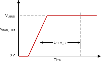
| tVBUS_DB | Debounce of VBUS_DET pin after valid VBUS_THR (See Figure 1.) | 2 | ms | ||
 Figure 1. VBUS Detect and Debounce