ZHCSE04D August 2015 – May 2017 TUSB320HI , TUSB320LI
PRODUCTION DATA.
- 1 特性
- 2 应用
- 3 说明
- 4 修订历史记录
- 5 Pin Configuration and Functions
- 6 Specifications
- 7 Detailed Description
- 8 Application and Implementation
- 9 Power Supply Recommendations
- 10Layout
- 11器件和文档支持
- 12机械、封装和可订购信息
8 Application and Implementation
NOTE
Information in the following applications sections is not part of the TI component specification, and TI does not warrant its accuracy or completeness. TI’s customers are responsible for determining suitability of components for their purposes. Customers should validate and test their design implementation to confirm system functionality.
8.1 Application Information
The TUSB320 device is a Type-C configuration channel logic and port controller. The TUSB320 device can detect when a Type-C device is attached, what type of device is attached, the orientation of the cable, and power capabilities (both detection and broadcast). The TUSB320 device can be used in a source application (DFP), in a sink application (UFP), or a combination source/sink application (DRP).
8.2 Typical Application
8.2.1 DRP in I2C Mode
Figure 10 and Figure 11 show a Type-C configuration for the DRP mode.
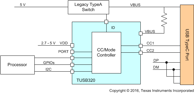 Figure 10. TUSB320 in DRP Mode Supporting Default Implementation
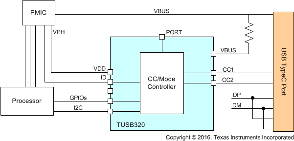 Figure 11. TUSB320 in DRP Mode Supporting Advanced Power Delivery
Figure 12 shows the TUSB320 device configured as a DRP in I2C mode.
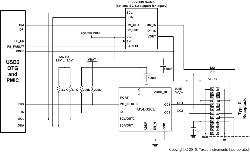 Figure 12. DRP in I2C Mode Schematic
8.2.1.1 Design Requirements
For this design example, use the parameters listed in Table 13:
Table 13. Design Requirements for DRP in I2C Mode
| DESIGN PARAMETER | VALUE |
|---|---|
| VDD (2.75 V to 5 V) | VBAT (less than 5 V) |
| Mode (I2C or GPIO) | I2C: ADDR pin must be pulled down or pulled up |
| I2C address (0x67 or 0x47) | 0x47: ADDR pin must be pulled low or tied to GND |
| Type-C port type (UFP, DFP, or DRP) | DRP: PORT pin is NC |
| Shutdown support | No |
8.2.1.2 Detailed Design Procedure
The TUSB320 device supports a VDD in the range of 2.75 V to 5 V. In this particular use case, VBAT which must be in the required VDD range is connected to the VDD pin. A 100-nF capacitor is placed near VDD.
The TUSB320 device is placed into I2C mode by either pulling the ADDR pin high or low. In this case, the ADDR pin is tied to GND which results in a I2C address of 0x47. The SDA and SCL must be pulled up to either 1.8 V or 3.3 V. When pulled up to 3.3 V, the VDD supply must be at least 3 V to keep from back-driving the I2C interface.
The TUSB320L device can enter shutdown mode by pulling the EN_N pin high, which puts the TUSB320L device into a low power state. In this case, external control of the EN_N pin is not implemented and therefore the EN_N pin is tied to GND. The TUSB320H device can enter shutdown mode by pulling the EN pin low, which puts the TUSB320H device into a low power state. In this case, external control of the EN pin is not implemented and therefore the EN pin is tied to 1.8V or 3.3V.
The INT_N/OUT3 pin is used to notify the PMIC when a change in the TUSB320 I2C registers occurs. This pin is an open drain output and requires an external pullup resistor. The pin should be pulled up to VDD using a 200-kΩ resistor.
The ID pin is used to indicate when a connection has occurred if the TUSB320 device is a DFP while configured for DRP. An OTG USB controller can use this pin to determine when to operate as a USB Host or USB Device. When this pin is driven low, the OTG USB controller functions as a host and then enables VBUS. The Type-C standard requires that a DFP not enable VBUS until it is in the Attached.SRC state. If the ID pin is not low but VBUS is detected, then OTG USB controller functions as a device. The ID pin is open drain output and requires an external pullup resistor. It should be pulled up to VDD using a 200-kΩ resistor.
The Type-C port mode is determined by the state of the PORT pin. When the PORT pin is not connected, the TUSB320 device is in DRP mode. The Type-C port mode can also be controlled by the MODE_SELECT register through the I2C interface.
The VBUS_DET pin must be connected through a 900-kΩ resistor to VBUS on the Type-C that is connected. This large resistor is required to protect the TUSB320 device from large VBUS voltage that is possible in present day systems. This resistor along with internal pulldown keeps the voltage observed by the TUSB320 device in the recommended range.
The USB2 specification requires the bulk capacitance on VBUS based on UFP or DFP. When operating the TUSB320 device in a DRP mode, it alternates between UFP and DFP. If the TUSB320 device connects as a UFP, the large bulk capacitance must be removed.
Table 14. USB2 Bulk Capacitance Requirements
| PORT CONFIGURATION | MIN | MAX | UNIT |
|---|---|---|---|
| Downstream facing port (DFP) | 120 | µF | |
| Upstream facing port (UFP) | 1 | 10 | µF |
8.2.1.3 Application Curves
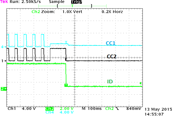 Figure 13. Application Curve for DRP in I2C Mode
8.2.2 DFP in I2C Mode
Figure 14 and Figure 15 show a Type-C configuration for the DFP mode.
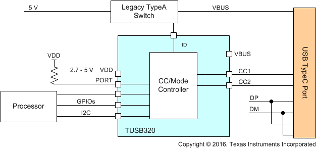 Figure 14. TUSB320 in DFP Mode Supporting Default Implementation
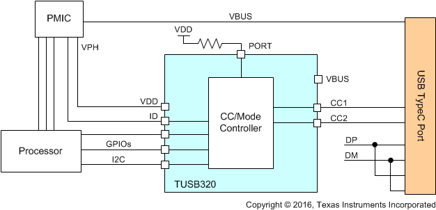 Figure 15. TUSB320 in DFP Mode Supporting Advanced Power Delivery
Figure 16 shows the TUSB320 device configured as a DFP in I2C mode.
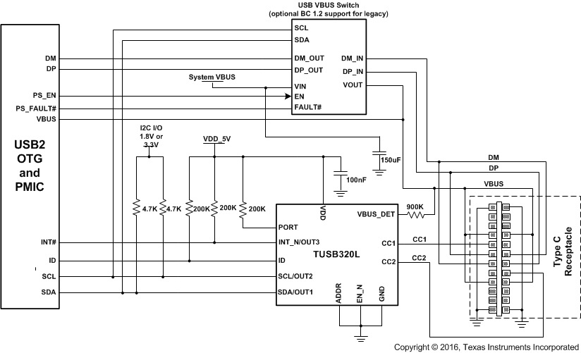 Figure 16. DFP in I2C Mode Schematic
8.2.2.1 Design Requirements
For this design example, use the parameters listed in Table 15:
Table 15. Design Requirements for DFP in I2C Mode
| DESIGN PARAMETER | VALUE |
|---|---|
| VDD (2.75 V to 5 V) | 5 V |
| Mode (I2C or GPIO) | I2C: ADDR pin must be pulled down or pulled up |
| I2C address (0x67 or 0x47) | 0x47: ADDR pin must be pulled low or tied to GND |
| Type-C port type (UFP, DFP, or DRP) | DFP: PORT pin is pulled up |
| Shutdown support | No |
8.2.2.2 Detailed Design Procedure
The TUSB320 device supports a VDD in the range of 2.75 V to 5 V. In this particular case, VDD is set to 5 V. A 100-nF capacitor is placed near VDD.
The TUSB320 device is placed into I2C mode by either pulling the ADDR pin high or low. In this particular case, the ADDR pin is tied to GND which results in a I2C address of 0x47. The SDA and SCL must be pulled up to either 1.8 V or 3.3 V. When pulled up to 3.3 V, the VDD supply must be at least 3 V to keep from back-driving the I2C interface.
The TUSB320L device can enter shutdown mode by pulling the EN_N pin high, which puts the TUSB320L device into a low power state. In this case, external control of the EN_N pin is not implemented and therefore the EN_N pin is tied to GND. The TUSB320H device can enter shutdown mode by pulling the EN pin low, which puts the TUSB320H device into a low power state. In this case, external control of the EN pin is not implemented and therefore the EN pin is tied to 1.8V or 3.3V.
The INT_N/OUT3 pin is used to notify the PMIC when a change in the TUSB320 I2C registers occurs. This pin is an open drain output and requires an external pullup resistor. The pin should be pulled up to VDD using a 200-kΩ resistor.
The Type-C port mode is determined by the state of the PORT pin. When the PORT pin is pulled high, the TUSB320 device is in DFP mode. The Type-C port mode can also be controlled by the MODE_SELECT register through the I2C interface.
The VBUS_DET pin must be connected through a 900-kΩ resistor to VBUS on the Type-C that is connected. This large resistor is required to protect the TUSB320 device from large VBUS voltage that is possible in present day systems. This resistor along with internal pulldown keeps the voltage observed by the TUSB320 device in the recommended range.
The USB2 specification requires the bulk capacitance on VBUS based on UFP or DFP. When operating the TUSB320 device in a DFP mode, a bulk capacitance of at least 120µF is required. In this particular case, a 150-µF capacitor was chosen.
8.2.2.3 Application Curves
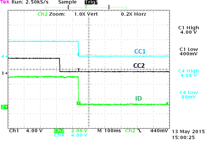 Figure 17. Application Curve for DFP in I2C Mode
8.2.3 UFP in I2C Mode
Figure 18 and Figure 19 show a Type-C configuration for the UFP mode.
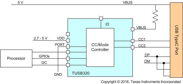 Figure 18. TUSB320 in UFP Mode Supporting Default Implementation
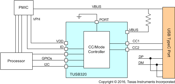 Figure 19. TUSB320 in UFP Mode Supporting Advanced Power Delivery
Figure 20 shows the TUSB320 device configured as a UFP in I2C mode.
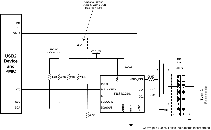 Figure 20. UFP in I2C Mode Schematic
8.2.3.1 Design Requirements
For this design example, use the parameters listed in Table 16:
Table 16. Design Requirements for UFP in I2C Mode
| DESIGN PARAMETER | VALUE |
|---|---|
| VDD (2.75 V to 5 V) | 5 V |
| Mode (I2C or GPIO) | I2C: ADDR pin must be pulled down or pulled up |
| I2C address (0x67 or 0x47) | 0x47: ADDR pin must be pulled low or tied to GND |
| Type-C port type (UFP, DFP, or DRP) | UFP: PORT pin is pulled down |
| Shutdown support | No |
8.2.3.2 Detailed Design Procedure
The TUSB320 device supports a VDD in the range of 2.75 V to 5 V. In this particular case, VDD is set to 5 V. A 100-nF capacitor is placed near VDD. If VBUS is guaranteed to be less than 5.5 V, powering the TUSB320 device through a diode can be implemented.
The TUSB320 device is placed into I2C mode by either pulling the ADDR pin high or low. In this case, the ADDR pin is tied to GND which results in a I2C address of 0x47. The SDA and SCL must be pulled up to either 1.8 V or 3.3 V. When pulled up to 3.3 V, the VDD supply must be at least 3 V to keep from back-driving the I2C interface.
The TUSB320L device can enter shutdown mode by pulling the EN_N pin high, which puts the TUSB320L device into a low power state. In this case, external control of the EN_N pin is not implemented and therefore the EN_N pin is tied to GND. The TUSB320H device can enter shutdown mode by pulling the EN pin low, which puts the TUSB320H device into a low power state. In this case, external control of the EN pin is not implemented and therefore the EN pin is tied to 1.8V or 3.3V.
The INT_N/OUT3 pin is used to notify the PMIC when a change in the TUSB320 I2C registers occurs. This pin is an open drain output and requires an external pullup resistor. The pin should be pulled up to VDD using a 200-kΩ resistor.
The Type-C port mode is determined by the state of the PORT pin. When the PORT pin is pulled low, the TUSB320 device is in UFP mode. The Type-C port mode can also be controlled by the MODE_SELECT register through the I2C interface.
The VBUS_DET pin must be connected through a 900-kΩ resistor to VBUS on the Type-C that is connected. This large resistor is required to protect the TUSB320 device from large VBUS voltage that is possible in present day systems. This resistor along with internal pulldown keeps the voltage observed by the TUSB320 device in the recommended range.
The USB2 specification requires the bulk capacitance on VBUS based on UFP or DFP. When operating the TUSB320 device in a UFP mode, a bulk capacitance between 1 to 10µF is required. In this particular case, a 1-µF capacitor was chosen.
8.2.3.3 Application Curves
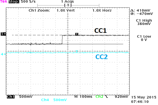 Figure 21. Application Curve for UFP in I2C Mode
8.3 Initialization Set Up
8.3.1 TUSB320L Initialization Procedure
The general power-up sequence for the TUSB320L device (EN_N tied to ground) is as follows:
- System is powered off (device has no VDD). The TUSB320L device is configured internally in UFP mode with Rds on CC pins (dead battery).
- VDD ramps – POR circuit. VDD must ramp within 25 ms or less. IO pull-up power rail (i.e. pull up on ID, INT, SCL, SDA, ADDR, PORT) must ramp with VDD or lag after VDD.
- I2C supply ramps up.
- The TUSB320L device enters unattached mode and determines the voltage level from the PORT pin. This determines the mode in which the TUSB320L device operates (DFP, UFP, DRP).
- The TUSB320L device monitors the CC pins as a DFP and VBUS for attach as a UFP.
- The TUSB320L device enters active mode when attach has been successfully detected.
8.3.2 TUSB320H Initialization Procedure
The general power-up sequence for the TUSB320H device (EN tied to 1.8V or 3.3V) is as follows:
- System is powered off (device has no VDD). The TUSB320H device is configured internally in UFP mode with Rds on CC pins (dead battery).
- VDD ramps – POR circuit. VDD must ramp within 25 ms or less. IO pull-up power rail (i.e. pull up on ID, INT, SCL, SDA, ADDR, PORT) must ramp with VDD or lag after VDD.
- I2C supply ramps up.
- The TUSB320H device enters unattached mode and determines the voltage level from the PORT pin. This determines the mode in which the TUSB320H device operates (DFP, UFP, DRP).
- The TUSB320H device monitors the CC pins as a DFP and VBUS for attach as a UFP.
- The TUSB320H device enters active mode when attach has been successfully detected.