ZHCSDT2C June 2015 – August 2018 TUSB321
PRODUCTION DATA.
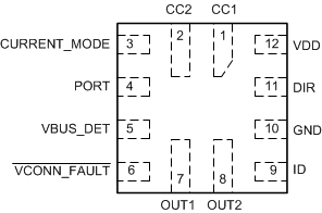
5 Pin Configuration and Functions
RWB Package
12-Pin X2QFN
Top View

Pin Functions
| PIN | TYPE | DESCRIPTION | |
|---|---|---|---|
| NAME | NO. | ||
| CC1 | 1 | I/O | Type-C configuration channel signal 1 |
| CC2 | 2 | I/O | Type-C configuration channel signal 2 |
| CURRENT_MODE | 3 | I | Advertise VBUS current. This 3-level input is used to control current advertisement in DFP mode or DRP mode connected as source. (See Table 2.)
L - Default Current. Pull-down to GND or leave unconnected. M - Medium (1.5A) current. Pull-up to VDD with 500-kΩ resistor. H - High (3.0A) current. Pull-up to VDD with 10-kΩ resistor. |
| PORT | 4 | I | Tri-level input pin to indicate port mode. The state of this pin is sampled when VDD is active.
H - DFP (Pull-up to VDD if DFP mode is desired) NC - DRP (Leave unconnected if DRP mode is desired) L - UFP (Pull-down or tie to GND if UFP mode is desired) |
| VBUS_DET | 5 | I | 5- to 28-V VBUS input voltage. VBUS detection determines UFP attachment. One RVBUS external resistor required between system VBUS and VBUS_DET pin. |
| VCONN_FAULT | 6 | O | Open-drain output and is asserted low for tFAULT when VCONN over-current fault is detected. (See Figure 2.) |
| OUT1 | 7 | I/O | This pin is an open drain output for communicating Type-C current mode detect when the device is in UFP mode. Default current mode detected (H); medium or high current mode detected (L). (See Table 2.) |
| OUT2 | 8 | I/O | This pin is an open drain output for communicating Type-C current mode detect when the device is in UFP mode: default or medium current mode detected (H); high current mode detected (L). (See Table 2.) |
| ID | 9 | O | Open drain output; asserted low when the CC pins detect device attachment when port is a source (DFP), or dual-role (DRP) acting as source (DFP). |
| GND | 10 | G | Ground |
| DIR | 11 | O | DIR of plug. This open drain output indicates the detected plug orientation: Type-C plug position 2 (H); Type-C plug position 1 (L). |
| VDD | 12 | P | Positive supply voltage |