ZHCSDZ1E July 2015 – July 2024 TUSB4020BI
PRODUCTION DATA
- 1
- 1 特性
- 2 应用
- 3 说明
- 4 Pin Configuration and Functions
- 5 Specifications
-
6 Detailed Description
- 6.1 Overview
- 6.2 Functional Block Diagram
- 6.3 Feature Description
- 6.4 Device Functional Modes
- 6.5 Programming
- 6.6
Register Maps
- 6.6.1
Configuration Registers
- 6.6.1.1 ROM Signature Register (offset = 0h) [reset = 0h]
- 6.6.1.2 Vendor ID LSB Register (offset = 1h) [reset = 51h]
- 6.6.1.3 Vendor ID MSB Register (offset = 2h) [reset = 4h]
- 6.6.1.4 Product ID LSB Register (offset = 3h) [reset = 25h]
- 6.6.1.5 Product ID MSB Register (offset = 4h) [reset = 80h]
- 6.6.1.6 Device Configuration Register (offset = 5h) [reset = 1Xh]
- 6.6.1.7 Battery Charging Support Register (offset = 6h) [reset = 0Xh]
- 6.6.1.8 Device Removable Configuration Register (offset = 7h) [reset = 0Xh]
- 6.6.1.9 Port Used Configuration Register (offset = 8h) [reset = 0h]
- 6.6.1.10 PHY Custom Configuration Register (offset = 9h) [reset = 0h]
- 6.6.1.11 Device Configuration Register 2 (offset = Ah)
- 6.6.1.12 UUID Registers (offset = 10h to 1Fh)
- 6.6.1.13 Language ID LSB Register (offset = 20h)
- 6.6.1.14 Language ID MSB Register (offset = 21h)
- 6.6.1.15 Serial Number String Length Register (offset = 22h)
- 6.6.1.16 Manufacturer String Length Register (offset = 23h)
- 6.6.1.17 Product String Length Register (offset = 24h)
- 6.6.1.18 Serial Number Registers (offset = 30h to 4Fh)
- 6.6.1.19 Manufacturer String Registers (offset = 50h to 8Fh)
- 6.6.1.20 Product String Registers (offset = 90h to CFh)
- 6.6.1.21 Additional Feature Configuration Register (offset = F0h)
- 6.6.1.22 Charging Port Control Register (offset = F2h)
- 6.6.1.23 Device Status and Command Register (offset = F8h)
- 6.6.1
Configuration Registers
-
7 Application and Implementation
- 7.1 Application Information
- 7.2 Typical Applications
- 7.3 Power Supply Recommendations
- 7.4 Layout
- 8 Device and Documentation Support
- 9 Revision History
- 10Mechanical, Packaging, and Orderable Information
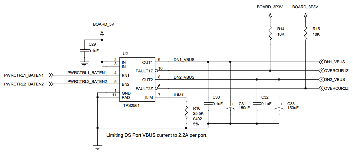
7.2.4 VBUS Power Switch Implementation
This particular example uses the TI TPS2561 dual-channel precision adjustable current-limited power switch. For details on this power switch or other power switches available from TI, refer to www.ti.com.
 Figure 7-7 Power Switch Implementation Schematic