ZHCSDY5C July 2015 – July 2024 TUSB4041I-Q1
PRODUCTION DATA
- 1
- 1 特性
- 2 应用
- 3 说明
- 4 Pin Configuration and Functions
- 5 Specifications
- 6 Detailed Description
-
7 Application and Implementation
- 7.1 Application Information
- 7.2
Typical Application
- 7.2.1 Design Requirements
- 7.2.2
Detailed Design Procedure
- 7.2.2.1 Upstream Port Implementation
- 7.2.2.2 Downstream Port 1 Implementation
- 7.2.2.3 Downstream Port 2 Implementation
- 7.2.2.4 Downstream Port 3 Implementation
- 7.2.2.5 Downstream Port 4 Implementation
- 7.2.2.6 VBUS Power Switch Implementation
- 7.2.2.7 Clock, Reset, and Miscellaneous
- 7.2.2.8 TUSB4041I-Q1 Power Implementation
- 7.2.3 Application Curves
- 7.3 Power Supply Recommendations
- 7.4 Layout
-
8 Register Maps
- 8.1 Configuration Registers
- 8.2 ROM Signature Register
- 8.3 Vendor ID LSB Register
- 8.4 Vendor ID MSB Register
- 8.5 Product ID LSB Register
- 8.6 Product ID MSB Register
- 8.7 Device Configuration Register
- 8.8 Battery Charging Support Register
- 8.9 Device Removable Configuration Register
- 8.10 Port Used Configuration Register
- 8.11 Device Configuration Register 2
- 8.12 USB 2.0 Port Polarity Control Register
- 8.13 UUID Byte N Register
- 8.14 Language ID LSB Register
- 8.15 Language ID MSB Register
- 8.16 Serial Number String Length Register
- 8.17 Manufacturer String Length Register
- 8.18 Product String Length Register
- 8.19 Serial Number String Registers
- 8.20 Manufacturer String Registers
- 8.21 Product String Byte N Register
- 8.22 Additional Feature Configuration Register
- 8.23 Device Status and Command Register
- 9 Device and Documentation Support
- 10Revision History
- 11Mechanical, Packaging, and Orderable Information
5.6 Power-Up Timing Requirements
| MIN | NOM | MAX | UNIT | ||
|---|---|---|---|---|---|
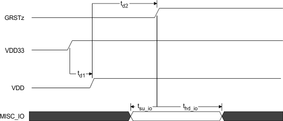
| td1 | VDD33 stable before VDD stable(1) | See (2) | ms | ||
| td2 | VDD and VDD33 stable before deassertion of GRSTz | 3 | ms | ||
| tsu_io | Setup for MISC inputs(3) sampled at the deassertion of GRSTz | 0.1 | µs | ||
| thd_io | Hold for MISC inputs(3) sampled at the deassertion of GRSTz | 0.1 | µs | ||
| tVDD33_RAMP | VDD33 supply ramp requirements | 0.2 | 100 | ms | |
| tVDD_RAMP | VDD supply ramp requirements | 0.2 | 100 | ms | |
(1) An active reset is required if the VDD33 supply is stable before the VDD11 supply. This active Reset shall meet the 3ms power-up delay counting from both power supplies being stable to the de-assertion of GRSTz.
(2) The VDD33 and VDD have no power-on relationship unless GRSTz is only connected to a capacitor to GND. Then VDD must be stable minimum of 10 μs before the VDD33.
(3) MISC pins sampled at de-assertion of GRSTz: FULLPWRMGMTz, GANGED, PWRCTL_POL, SMBUSz, BATEN[4:1], and AUTOENz.
 Figure 5-1 Power-Up Timing Requirements