ZHCSDY6E July 2015 – September 2017 TUSB4041I
PRODUCTION DATA.
- 1 特性
- 2 应用
- 3 说明
- 4 修订历史记录
- 5 说明 (续)
- 6 Pin Configuration and Functions
- 7 Specifications
-
8 Detailed Description
- 8.1 Overview
- 8.2 Functional Block Diagram
- 8.3 Feature Description
- 8.4 Device Functional Modes
- 8.5
Register Maps
- 8.5.1 Configuration Registers
- 8.5.2 ROM Signature Register
- 8.5.3 Vendor ID LSB Register
- 8.5.4 Vendor ID MSB Register
- 8.5.5 Product ID LSB Register
- 8.5.6 Product ID MSB Register
- 8.5.7 Device Configuration Register
- 8.5.8 Battery Charging Support Register
- 8.5.9 Device Removable Configuration Register
- 8.5.10 Port Used Configuration Register
- 8.5.11 Device Configuration Register 2
- 8.5.12 USB 2.0 Port Polarity Control Register
- 8.5.13 UUID Byte N Register
- 8.5.14 Language ID LSB Register
- 8.5.15 Language ID MSB Register
- 8.5.16 Serial Number String Length Register
- 8.5.17 Manufacturer String Length Register
- 8.5.18 Product String Length Register
- 8.5.19 Serial Number String Registers
- 8.5.20 Manufacturer String Registers
- 8.5.21 Product String Byte N Register
- 8.5.22 Additional Feature Configuration Register
- 8.5.23 Device Status and Command Register
-
9 Application and Implementation
- 9.1 Application Information
- 9.2
Typical Application
- 9.2.1 Design Requirements
- 9.2.2
Detailed Design Procedure
- 9.2.2.1 Upstream Port Implementation
- 9.2.2.2 Downstream Port 1 Implementation
- 9.2.2.3 Downstream Port 2 Implementation
- 9.2.2.4 Downstream Port 3 Implementation
- 9.2.2.5 Downstream Port 4 Implementation
- 9.2.2.6 VBUS Power Switch Implementation
- 9.2.2.7 Clock, Reset, and Miscellaneous
- 9.2.2.8 TUSB4041I Power Implementation
- 9.2.3 Application Curves
- 10Power Supply Recommendations
- 11Layout
- 12器件和文档支持
- 13机械、封装和可订购信息
9 Application and Implementation
NOTE
Information in the following applications sections is not part of the TI component specification, and TI does not warrant its accuracy or completeness. TI’s customers are responsible for determining suitability of components for their purposes. Customers should validate and test their design implementation to confirm system functionality.
9.1 Application Information
The TUSB4041I device is a four-port USB 2.0 hub. The provides USB high-speed and full-speed connections on the upstream port and provides USB high-speed, full-speed, or low-speed connections on the downstream port. The TUSB4041I device can be used in any application that requires additional USB-compliant ports. For example, a specific notebook may only have two downstream USB ports. By using the TUSB4041I device, the notebook can increase the downstream port count to five.
9.2 Typical Application
A common application for the TUSB4041I device is as a self-powered standalone USB-hub product. The product is powered by an external 5-V DC power adapter. In this application, using a USB cable, the upstream port of the TUSB4041I device is plugged into a USB host controller. The downstream ports of the TUSB4041I device are exposed to users for connecting USB hard drives, cameras, flash drives, and so forth.
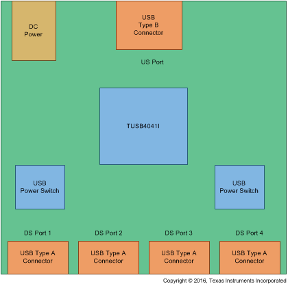 Figure 25. Discrete USB Hub Product
9.2.1 Design Requirements
For this design example, use the parameters listed in Table 26.
Table 26. Design Parameters
| DESIGN PARAMETER | EXAMPLE VALUE |
|---|---|
| VDD supply | 1.1 V |
| VDD33 supply | 3.3 V |
| Upstream port USB support (HS, FS) | HS, FS |
| Downstream port 1 USB support (HS, FS, LS) | HS, FS, LS |
| Downstream port 2 USB support (HS, FS, LS) | HS, FS, LS |
| Downstream port 3 USB support (HS, FS, LS) | HS, FS, LS |
| Downstream port 4 USB support (HS, FS, LS) | HS, FS, LS |
| Number of removable downstream ports | 4 |
| Number of non-removable downstream ports | 0 |
| Full power management of downstream ports | Yes (FULLPWRMGMTZ = 0) |
| Individual control of downstream port power switch | Yes (GANGED = 0) |
| Power switch enable polarity | Active high (PWRCTL_POL = 1) |
| Battery charge support for downstream port 1 | Yes |
| Battery charge support for downstream port 2 | Yes |
| Battery charge support for downstream port 3 | Yes |
| Battery charge support for downstream port 4 | Yes |
| I2C EEPROM support | No |
| 24-MHz clock source | Crystal |
9.2.2 Detailed Design Procedure
9.2.2.1 Upstream Port Implementation
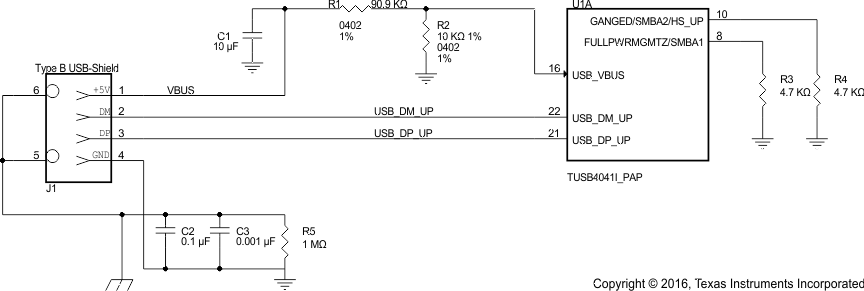 Figure 26. Upstream Port Implementation
The upstream of the TUSB4041I device is connected to a USB2 Type B connector. This particular example has GANGED pin and FULLPWRMGMTZ pin pulled low, which results in individual power support each downstream port. The VBUS signal from the USB2 Type B connector is feed through a voltage divider. The purpose of the voltage divider is to make sure the level meets USB_VBUS input requirements
9.2.2.2 Downstream Port 1 Implementation
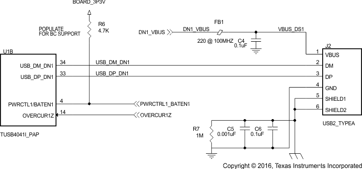 Figure 27. Downstream Port 1 Implementation
The downstream port 1 of the TUSB4041I device is connected to a USB2 type A connector. With BATEN1 pin pulled up, battery charge support is enabled for Port 1. If battery charge support is not needed, then uninstall the pullup resistor on BATEN1.
9.2.2.3 Downstream Port 2 Implementation
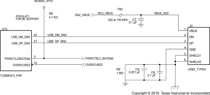 Figure 28. Downstream Port 2 Implementation
The downstream port 2 of the TUSB4041I device is connected to a USB2 type A connector. With BATEN2 pin pulled up, battery charge support is enabled for port 2. If battery charge support is not needed, then uninstall the pullup resistor on BATEN2.
9.2.2.4 Downstream Port 3 Implementation
 Figure 29. Downstream Port 3 Implementation
The downstream port3 of the TUSB4041I device is connected to a USB2 type A connector. With BATEN3 pin pulled up, battery charge support is enabled for port 3. If battery charge support is not needed, then uninstall the pullup resistor on BATEN3.
9.2.2.5 Downstream Port 4 Implementation
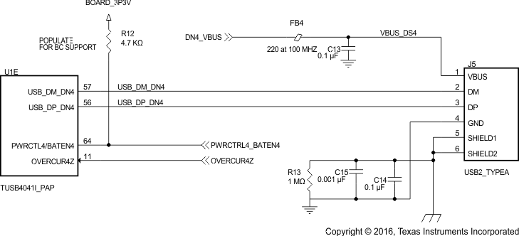 Figure 30. Downstream Port 4 Implementation
The downstream port 4 of the TUSB4041I device is connected to a USB2 Type A connector. With BATEN4 pin pulled up, Battery Charge support is enabled for Port 4. If Battery Charge support is not needed, then uninstall the pullup resistor on BATEN4.
9.2.2.6 VBUS Power Switch Implementation
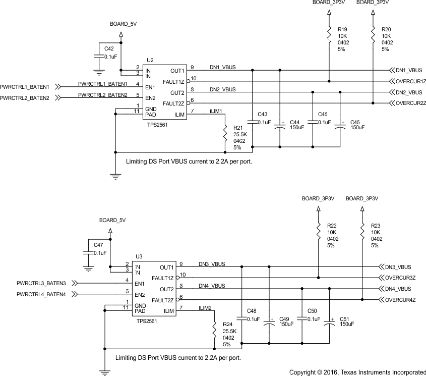 Figure 31. VBUS Power Switch Implementation
This particular example uses TI's TPS2561 dual-channel precision adjustable current-limited power switch. For details on this power switch or other power switches available from TI, refer to www.ti.com.
9.2.2.7 Clock, Reset, and Miscellaneous
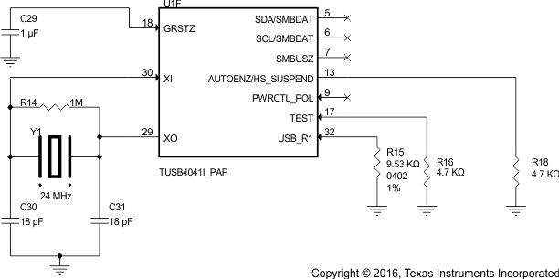
The PWRCTL_POL is left unconnected which results in active-high power enable (PWRCTL1, PWRCTL2, PWRCTL3, and PWRCTL4) for a USB VBUS power switch. The 1-µF capacitor on the GRSTN pin can only be used if the VDD11 supply is stable before the VDD33 supply. Depending on the supply ramp of the two supplies, the user may need to adjust the capacitor.
9.2.2.8 TUSB4041I Power Implementation
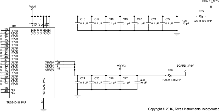 Figure 33. TUSB4041I Power Implementation
9.2.3 Application Curves
