ZHCSFQ2C November 2016 – June 2018 TUSB422
PRODUCTION DATA.
- 1 特性
- 2 应用
- 3 说明
- 4 修订历史记录
- 5 Pin Configuration and Functions
- 6 Specifications
-
7 Detailed Description
- 7.1 Overview
- 7.2 Functional Block Diagram
- 7.3
Feature Description
- 7.3.1 USB PD I2C Type-C Port Controller Interface (TCPC)
- 7.3.2 USB PD BMC PHY
- 7.3.3 DFP (Downstream Facing Port)
- 7.3.4 UFP (Upstream Facing Port)
- 7.3.5 DRP (Dual-Role Port)
- 7.3.6 Type-C Current Mode Advertising
- 7.3.7 VBUS Source Enable/Disable Control
- 7.3.8 VBUS Sink Enable/Disable Control
- 7.3.9 VBUS Monitoring
- 7.3.10 VBUS Discharge
- 7.3.11 VBUS to CC Short Detection from Legacy Charger
- 7.3.12 VBUS Power Source Requirements
- 7.3.13 VBUS Power Sink Requirements.
- 7.3.14 VCONN
- 7.3.15 Interrupts
- 7.3.16 Fast Role Swap
- 7.4 Device Functional Modes
- 7.5 Programming
- 7.6
Register Maps
- 7.6.1 CSR Registers
- 7.6.2 Vendor ID Byte 0 Register (address = 0x00) [reset = 0x51]
- 7.6.3 Vendor ID Byte 1 Register (address = 0x01) [reset = 0x04]
- 7.6.4 Product ID Byte 0 Register (address = 0x02) [reset = 0x22]
- 7.6.5 Product ID Byte 1 Register (address = 0x03) [reset = 0x04]
- 7.6.6 Device ID Byte 0 Register (address = 0x04) [reset = 0x00]
- 7.6.7 Device ID Byte 1 Register (address = 0x05) [reset = 0x01]
- 7.6.8 USB Type-C Revision Byte 0 Register (address = 0x06) [reset = 0x11]
- 7.6.9 USB Type-C Revision Byte 1 Register (address = 0x07) [reset = 0x00]
- 7.6.10 USB PD Revision Version Byte 0 Register (address = 0x08) [reset = 0x11]
- 7.6.11 USB PD Revision Version Byte 1 Register (address = 0x09) [reset = 0x20]
- 7.6.12 PD Interface Revision Byte 0 Register (address = 0x0A) [reset = 0x10]
- 7.6.13 PD Interface Revision Byte 1 Register (address = 0x0B) [reset = 0x10]
- 7.6.14 Alert Byte 0 Register (address = 0x10) [reset = 0x00]
- 7.6.15 Alert Byte 1 Register (address = 0x11) [reset = 0x00]
- 7.6.16 Alert Mask Byte 0 Register (address = 0x12) [reset = 0xFFh]
- 7.6.17 Alert Mask Byte 1 Register (address = 0x13) [reset = 0x0F]
- 7.6.18 Power Status Mask Register (address = 0x14) [reset = 0xFF]
- 7.6.19 FAULT Status Mask Register (address = 0x15) [reset = 0x7F]
- 7.6.20 Config Standard Output Register (address = 0x18) [reset = 0x60]
- 7.6.21 TCPC Control Register (address = 0x19) [reset = 0x00]
- 7.6.22 ROLE Control Register (address = 0x1A) [reset = 0x0A]
- 7.6.23 FAULT Control Register (address = 0x1B) [reset = 0x06]
- 7.6.24 Power Control Register (address = 0x1C) [reset = 0x60]
- 7.6.25 CC Status Register (address = 0x1D) [reset = 0x00]
- 7.6.26 Power Status Register (address = 0x1E) [reset = 0x00]
- 7.6.27 Fault Status Register (address = 0x1F) [reset = 0x00]
- 7.6.28 Command Register (address = 0x23) [reset = 0x00]
- 7.6.29 Device Capabilities 1 Byte 0 Register (address = 0x24) [reset = 0x98]
- 7.6.30 Device Capabilities 1 Byte 1 Register (address = 0x25) [reset = 0x1E]
- 7.6.31 Device Capabilities 2 Byte 0 Register (address = 0x26) [reset = 0xC5]
- 7.6.32 Device Capabilities 2 Byte 1 Register (address = 0x27) [reset = 0x00]
- 7.6.33 Standard Input Capabilities Register (address = 0x28) [reset = 0x00]
- 7.6.34 Standard Output Capabilities Register (address = 0x29) [reset = 0x00]
- 7.6.35 Message Header Info Register (address = 0x2E) [reset = 0x02]
- 7.6.36 Receiver Detect Register (address = 0x2F) [reset = 0x00]
- 7.6.37 Receive Byte Count Register (address = 0x30) [reset = 0x00]
- 7.6.38 Receive Buffer Frame Type Register (address = 0x31) [reset = 0x00]
- 7.6.39 Receive Buffer Header Byte 0 Register (address = 0x32) [reset = 0x00]
- 7.6.40 Receive Buffer Header Byte 1 Register (address = 0x33) [reset = 0x00]
- 7.6.41 Receive Buffer Data Object 1 Through 7 Register (address = 0x34 through 0x4F) [reset = 0x00]
- 7.6.42 Transmit Register (address = 0x50) [reset = 0x00]
- 7.6.43 Transmit Byte Count Register (address = 0x51) [reset = 0x00]
- 7.6.44 Transmit Buffer Header Byte 0 Register (address = 0x52) [reset = 0x00]
- 7.6.45 Transmit Buffer Header Byte 1 Register (address = 0x53) [reset = 0x00]
- 7.6.46 Transmit Buffer Data Object 1 Through 7 Register (address = 0x54 through 0x6F) [reset = 0x00]
- 7.6.47 VBUS Voltage Byte 0 Register (address = 0x70) [reset = 0x00]
- 7.6.48 VBUS Voltage Byte 1 Register (address = 0x71) [reset = 0x00]
- 7.6.49 VBUS Sink Disconnect Threshold Byte 0 Register (address = 0x72) [reset = 0x00]
- 7.6.50 VBUS Sink Disconnect Threshold Byte 1 Register (address = 0x73) [reset = 0x00]
- 7.6.51 VBUS Stop Discharge Threshold Byte 0 Register (address = 0x74) [reset = 0x00]
- 7.6.52 VBUS Stop Discharge Threshold Byte 1 Register (address = 0x75) [reset = 0x00]
- 7.6.53 VBUS Voltage Alarm High Config Byte 0 Register (address = 0x76) [reset = 0x00]
- 7.6.54 VBUS Voltage Alarm High Config Byte 1 Register (address = 0x77) [reset = 0x00]
- 7.6.55 VBUS Voltage Alarm Low Config Byte 0 Register (address = 0x78) [reset = 0x00]
- 7.6.56 VBUS Voltage Alarm Low Config Byte 1 Register (address = 0x79) [reset = 0x00]
- 7.6.57 Vendor Interrupts Status Register (address = 0x90) [reset = 0x00]
- 7.6.58 Vendor Interrupts Mask Register (address = 0x92) [reset = 0x00]
- 7.6.59 CC General Control Register (address = 0x94) [reset = 0x04]
- 7.6.60 PHY BMC TX Control Register (address = 0x95) [reset = 0x00]
- 7.6.61 PHY BMC RX Control Register (address = 0x96) [reset = 0x00]
- 7.6.62 PHY BMC RX Status Register (address = 0x97) [reset = 0x00]
- 7.6.63 VBUS and VCONN Control Register (address = 0x98) [reset = 0x00]
- 7.6.64 OTSD Control Register (address = 0x99) [reset = 0x00]
- 7.6.65 LFO Timer Low Register (address = 0xA0) [reset = 0x00]
- 7.6.66 LFO Timer High Register (address = 0xA1) [reset = 0x00]
- 7.6.67 Page Select Register (address = 0xFF) [reset = 0x00]
- 8 Application and Implementation
- 9 Power Supply Recommendations
- 10Layout
- 11器件和文档支持
- 12机械、封装和可订购信息
Device Images
空白
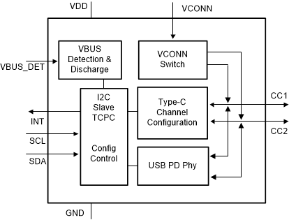
简化电路原理图

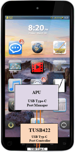
USB Type-C 智能手机
