ZHCSFL6E July 2016 – November 2023 TUSB522P
PRODUCTION DATA
- 1
- 1 特性
- 2 应用
- 3 说明
- 4 Revision History
- 5 Pin Configuration and Functions
- 6 Specifications
- 7 Detailed Description
- 8 Application and Implementation
- 9 Device and Documentation Support
- 10Mechanical, Packaging, and Orderable Information
5 Pin Configuration and Functions
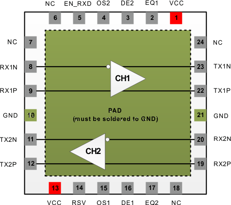
 Figure 5-1 RGE Package, 24-Pin (VQFN)
(Top View)
Figure 5-1 RGE Package, 24-Pin (VQFN)
(Top View)Table 5-1 Pin Functions
| PIN | I/O | DESCRIPTION | |
|---|---|---|---|
| NAME | NO. | ||
| RX1N | 8 | Differential I | Differential input for 5Gbps negative signal on Channel 1 |
| RX1P | 9 | Differential I | Differential input for 5Gbps positive signal on Channel 1 |
| TX1N | 23 | Differential O | Differential output for 5Gbps negative signal on Channel 1 |
| TX1P | 22 | Differential O | Differential output for 5Gbps positive signal on Channel 1 |
| RX2N | 20 | Differential I | Differential input for 5Gbps negative signal on Channel 2 |
| RX2P | 19 | Differential I | Differential input for 5Gbps positive signal on Channel 2 |
| TX2N | 11 | Differential O | Differential output for 5Gbps negative signal on Channel 2 |
| TX2P | 12 | Differential O | Differential output for 5Gbps positive signal on Channel 2 |
| EQ1 | 2 | I, CMOS | Sets the receiver equalizer gain for Channel 1. 3-state input with
integrated pull-up and pull-down resistors. EQ1 = Low = 3 dB EQ1 = Mid = 6 dB EQ1 = High = 9 dB |
| DE1 | 16 | I, CMOS | Sets the output de-emphasis for Channel 1. 3-state input with
integrated pull-up and pull-down resistors. DE1 = Low = 0 dB DE1 = Mid = -3.5 dB DE1 = High = -6.2 dB |
| OS1 | 15 | I, CMOS | Sets the output swing (differential voltage amplitude) for Channel
1. 2-state input with an integrated pull down resistor. OS1 = Low = 0.9 mV OS1 = High = 1.1 mV |
| EQ2 | 17 | I, CMOS | Sets the receiver equalizer gain for Channel 2. 3-state input with
integrated pull-up and pull-down resistors. EQ2 = Low = 3 dB EQ2 = Mid = 6 dB EQ2 = High = 9 dB |
| DE2 | 3 | I, CMOS | Sets the output de-emphasis for Channel 2. 3-state input with
integrated pull-up and pull-down resistors. DE2 = Low = 0 dB DE2 = Mid = -3.5 dB DE2 = High = -6.2 dB |
| OS2 | 4 | I, CMOS | Sets the output swing (differential voltage amplitude) for Channel
2. 2-state input with an integrated pull down resistor. OS2 = Low = 0.9 mV OS2 = High = 1.1 mV |
| EN_RXD | 5 | I, CMOS | Enable. The device has a 660-kΩ pulldown resistor. Device is active when EN_RXD = High. Drive actively high or install a pullup resistor (recommend 4.7 KΩ) for normal operation. Does reset state machine. |
| RSV | 14 | I, CMOS | Reserved. Can be left as no-connect. |
| VCC | 1, 13 | P | Positive power supply. Power supply is 3.3 V. |
| GND | 10, 21, PAD | G | Ground. PAD must be connected to Ground. Pins 10, 21 can be connected to Ground or left unconnected. |
| NC | 6, 7, 18, 24 | — | No connection. These pins can be tied to any desired voltages including connecting them to GND. |