ZHCSGZ9G October 2017 – November 2022 TUSB564
PRODUCTION DATA
- 1 特性
- 2 应用
- 3 说明
- 4 Revision History
- 5 Pin Configuration and Functions
- 6 Specifications
- 7 Parameter Measurement Information
-
8 Detailed Description
- 8.1 Overview
- 8.2 Functional Block Diagram
- 8.3 Feature Description
- 8.4 Device Functional Modes
- 8.5 Programming
- 8.6
Register Maps
- 8.6.1 General Register (address = 0x0A) [reset = 00000001]
- 8.6.2 DisplayPort Control/Status Registers (address = 0x10) [reset = 00000000]
- 8.6.3 DisplayPort Control/Status Registers (address = 0x11) [reset = 00000000]
- 8.6.4 DisplayPort Control/Status Registers (address = 0x12) [reset = 00000000]
- 8.6.5 DisplayPort Control/Status Registers (address = 0x13) [reset = 00000000]
- 8.6.6 USB3.1 Control/Status Registers (address = 0x20) [reset = 00000000]
- 8.6.7 USB3.1 Control/Status Registers (address = 0x21) [reset = 00000000]
- 8.6.8 USB3.1 Control/Status Registers (address = 0x22) [reset = 00000000]
- 9 Application and Implementation
- 10Power Supply Recommendations
- 11Layout
- 12Device and Documentation Support
- 13Mechanical, Packaging, and Orderable Information
9.3.2 USB 3.1 and 2 Lanes of DisplayPort
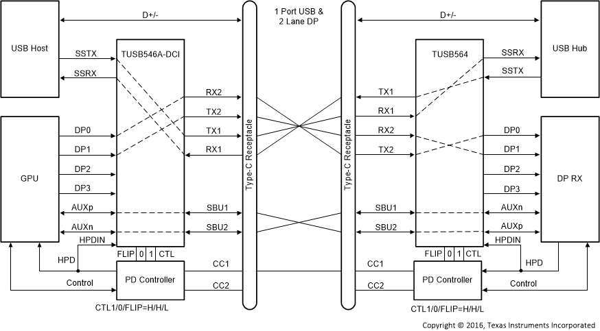
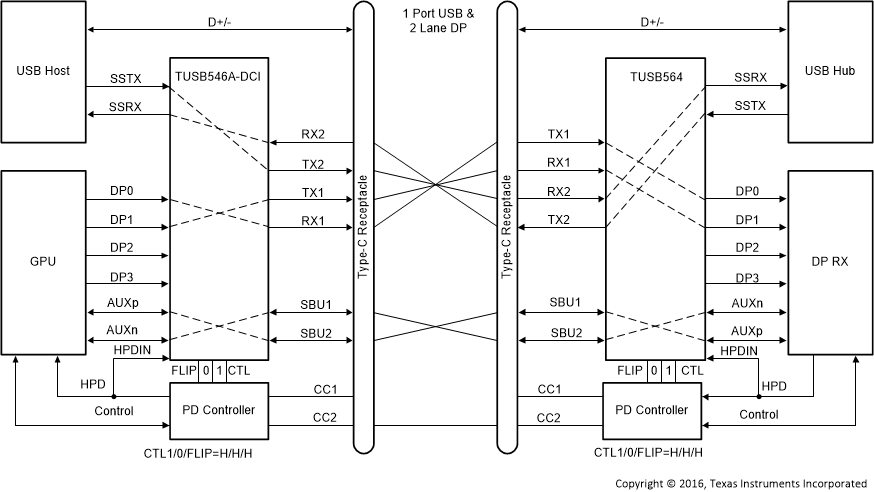
The TUSB564 operates in USB3.1 and 2 Lanes of DisplayPort mode when the CTL1 pin is high and CTL0 pin is high.
 Figure 9-8 USB3.1 + 2 Lane DP – No Flip (CTL1 = H, CTL0 = H, FLIP = L)
 Figure 9-9 USB 3.1 + 2 Lane DP – Flip (CTL1 = H, CTL0 = H, FLIP = H)