ZHCSKL2A December 2019 – May 2022 TUSS4470
PRODUCTION DATA
- 1 特性
- 2 应用
- 3 说明
- 4 Revision History
- 5 Pin Configuration and Functions
-
6 Specifications
- 6.1 Absolute Maximum Ratings
- 6.2 ESD Ratings
- 6.3 Recommended Operating Conditions
- 6.4 Thermal Information
- 6.5 Power-Up Characteristics
- 6.6 Transducer Drive
- 6.7 Receiver Characteristics
- 6.8 Echo Interrupt Comparator Characteristics
- 6.9 Digital I/O Characteristics
- 6.10 Switching Characteristics
- 6.11 Typical Characteristics
- 7 Detailed Description
- 8 Application and Implementation
- 9 Power Supply Recommendations
- 10Layout
- 11Device and Documentation Support
- 12Mechanical, Packaging, and Orderable Information
7.3.2 Burst Generation
TUSS4470 has multiple modes to excite the transducer through OUTA and OUTB pins. For each of the modes, the desired frequency of burst is supplied through an external clock on the IOx pins. This enables the user to supply a highly precise clock calibrated to the center frequency of transducer to enable the highest sound pressure level generation. These modes can be selected by the IO_MODE bits in the DEV_CTRL_3 register.
The burst mode is enabled first, then the start of burst (OUTA/OUTB changing states) happens at the next falling edge of IO1 or IO2, depending on the mode selected. These modes are described below.
- IO_MODE = 0: In this mode, the external clock for the transducer
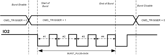
is applied at the IO2 pin and the burst mode is enabled by setting the CMD_TRIGGER in the TOF_CONFIG register through SPI, as shown in Figure 7-1. The device then expects a clock at IO2 pin to generate pulses on the OUTA/OUTB pins.
The start of burst happens from the first falling edge of IO2. The number of pulses are
counted by counting falling edge to next falling edge transitions on IO2 once the start of
burst is triggered. The end of burst sequence is signaled when the number of pulses
defined in BURST_PULSE are sent, or when the CMD_TRIGGER = 0 is set through SPI, whichever occurs earlier. TI recommends that
IO2 is held high before burst enable to count the number of pulses correctly. After the
start of burst, the state of OUTA and OUTB pins are determined by IO1 and IO2 pins. A
transition of CMD_TRIGGER from high to low to high again is required to initiate a new
burst sequence.
 Figure 7-1 IO_MODE 0 Description
 - IO_MODE = 1: In this mode, the external clock for the transducer
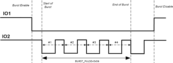
is applied at the IO2 pin and the burst mode is enabled when IO1 pin transitions low (see
Figure 7-2). The device then expects a clock at IO2 pin to generate pulses on the OUTA/OUTB pins.
The start of burst happens from the first falling edge of IO2. The number of pulses are
counted by counting falling edge to next falling edge transitions on IO2 once the start of
burst is triggered. End of burst sequence is signaled when the number of pulses defined in
BURST_PULSE are sent or IO1 transitions high, whichever occurs earlier. TI
recommends that IO2 is held high before start of burst to count the number of pulse
correctly. After the start of burst, the state of OUTA and OUTB pins are determined by IO1
and IO2 pins. A transition of IO1 from low to high to low again is required to initiate a
new burst sequence.
 Figure 7-2 IO_MODE 1 Description
 - IO_MODE = 2: In this mode both IO1 and IO2 are used to control
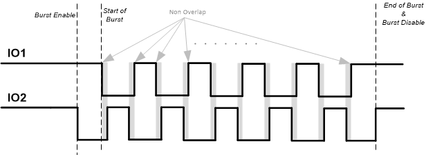
OUTA and OUTB. The burst enable is triggered when either IO1 or IO2 transitions from high
to low. Start of burst (OUTA and OUTB changing state) happens only at the next falling
edge of IO1. Figure 7-3 shows the case where a high-to-low transition on IO2 is used to enable the burst. A
burst is emulated when IO1 and IO2 are toggled in a non-overlapping sequence. After the
start of burst, the state of OUTA and OUTB pins are determined by IO1 and IO2 pins. During
a burst, if there is a condition where both IO1 and IO2 are high for more than half period
of the internal clock fINT_CLK (caused by differential delays due to PCB
parasitics or MCU code), an end of burst and burst mode disable will be triggered. Any
falling edge just after this condition will be ignored to toggle OUTA and OUTB as it would
be considered as a new burst enable signal. A systematic condition of overlap can cause a
continuous end of burst trigger such that OUTA and OUTB do not toggle even though IO1 and
IO2 are toggling. TI recommends no overlap or minimum non-overlap between the IO1 and IO2
signals when measured at the pins. BURST_PULSE has no effect in this mode.
 Figure 7-3 IO_MODE 2 Description
 - IO_MODE = 3: In this mode, burst enable and start of burst are
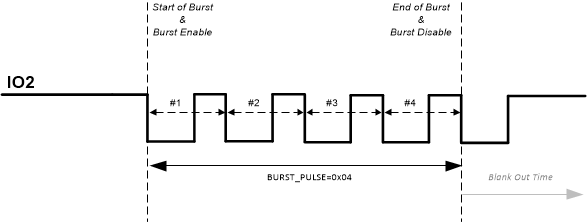
both triggered by the falling edge of IO2. TI recommends that IO2 pin is kept pulled up to
VDD for this mode. The device then expects a clock at IO2 pin to generate pulses on the
OUTA/OUTB pins (see Figure 7-4). The number of pulses are counted by counting falling edge to next falling edge
transitions on IO2 once the start of burst is triggered. End of burst sequence is signaled
when the number of pulses defined in BURST_PULSE are sent. After end of burst, a blank-out timer interval defined by
the DRV_PLS_FLT_DT register is started to prevent triggering of a new start of burst
in the event if the IO2 pin is still toggling. After the start of burst, the state of OUTA
and OUTB pins are determined by IO1 and IO2 pins.
 Figure 7-4 IO_MODE 3 Description
- For IO_MODE 0 and 1, by setting BURST_PULSE = 0, the device will generate continuous burst pulses on OUTA and OUTB until the end of burst is signaled through SPI or the IO1 pin, respectively. Continuous bursting is not available for IO_MODE=3.
- A higher noise floor at the VOUT pin is expected in continuous mode where one transducer is used to transmit burst signals and another transducer is used to receive, as the switching noise of the digital IO pins can couple into the highly sensitive analog front end for the receive channel. This also applies to the single transducer use case where a continuous clock is applied on IO2 pin when the device is in indirect or listening mode.
- The range for frequency of switching for the output drivers is given by fDRV_CLK parameter in the Switching Characteristics table.
- When the device is not in direct sensing or bursting mode, the device is always in indirect sensing or listening mode.