ZHCSI11A August 2009 – April 2018 TXB0106-Q1
PRODUCTION DATA.
- 1 特性
- 2 应用
- 3 说明
- 4 修订历史记录
- 5 Pin Configuration and Functions
-
6 Specifications
- 6.1 Absolute Maximum Ratings
- 6.2 ESD Ratings
- 6.3 Recommended Operating Conditions
- 6.4 Thermal Information
- 6.5 Electrical Characteristics
- 6.6 Timing Requirements – VCCA = 1.2 V, TA = 25°C
- 6.7 Timing Requirements – VCCA = 1.5 V ± 0.1 V
- 6.8 Timing Requirements – VCCA = 1.8 V ± 0.15 V
- 6.9 Timing Requirements – VCCA = 2.5 V ± 0.2 V
- 6.10 Timing Requirements – VCCA = 3.3 V ± 0.3 V
- 6.11 Switching Characteristics –VCCA = 1.2 V, TA = 25°C
- 6.12 Switching Characteristics – VCCA = 1.5 V ± 0.1 V
- 6.13 Switching Characteristics – VCCA = 1.8 V ± 0.15 V
- 6.14 Switching Characteristics – VCCA = 2.5 V ± 0.2 V
- 6.15 Switching Characteristics – VCCA = 3.3 V ± 0.3 V
- 6.16 Operating Characteristics
- 6.17 Typical Characteristics
- 7 Parameter Measurement Information
- 8 Detailed Description
- 9 Application and Implementation
- 10Power Supply Recommendations
- 11Layout
- 12器件和文档支持
- 13机械、封装和可订购信息
8.3.1 Architecture
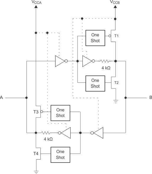
The TXB0106-Q1 architecture (see Figure 5) does not require a direction-control signal to control the direction of data flow from A to B or from B to A. In a dc state, the output drivers of the TXB0106-Q1 device can maintain a high or low, but are designed to be weak, so that they can be overdriven by an external driver when data on the bus starts flowing in the opposite direction.
The output one-shots detect rising or falling edges on the A or B ports. During a rising edge, the one-shot turns on the PMOS transistors (T1, T3) for a short duration, which speeds up the low-to-high transition. Similarly, during a falling edge, the one-shot turns on the NMOS transistors (T2, T4) for a short duration, which speeds up the high-to-low transition. The typical output impedance during output transition is 70 Ω at VCCO = 1.2 V to 1.8 V, 50 Ω at VCCO = 1.8 V to 3.3 V, and 40 Ω at VCCO = 3.3 V to 5 V.
 Figure 5. Architecture of the TXB0106-Q1 I/O Cell