SCES638D October 2007 – June 2017 TXS0101
PRODUCTION DATA.
- 1 Features
- 2 Applications
- 3 Description
- 4 Revision History
- 5 Pin Configuration and Functions
-
6 Specifications
- 6.1 Absolute Maximum Ratings
- 6.2 ESD Ratings
- 6.3 Recommended Operating Conditions
- 6.4 Thermal Information
- 6.5 Electrical Characteristics
- 6.6 Timing Requirements: V CCA = 1.8 V ± 0.15 V
- 6.7 Timing Requirements VCCA = 2.5 V ± 0.2 V
- 6.8 Timing Requirements: 3.3 V ± 0.3 V
- 6.9 Switching Characteristics: VCCA = 1.8 V ± 0.15 V
- 6.10 Switching Characteristics: VCCA = 2.5 V ± 0.2 V
- 6.11 Switching Characteristics: VCCA = 3.3 V ± 0.3 V
- 6.12 Typical Characteristics
- 7 Parameter Measurement Information
- 8 Detailed Description
- 9 Application and Implementation
- 10Power Supply Recommendations
- 11Layout
- 12Device and Documentation Support
- 13Mechanical, Packaging, and Orderable Information
封装选项
机械数据 (封装 | 引脚)
散热焊盘机械数据 (封装 | 引脚)
订购信息
8 Detailed Description
8.1 Overview
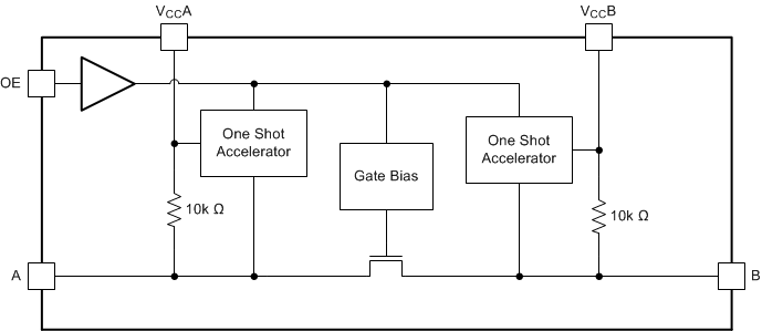
The TXS0101 device is a directionless voltage-level translator specifically designed for translating logic voltage levels. The A port is able to accept I/O voltages ranging from 1.65 V to 3.6 V, while the B port can accept I/O voltages from 2.3 V to 5.5 V. The device is a pass gate architecture with edge rate accelerators (one shots) to improve the overall data rate. 10 kΩ pullup resistors, commonly used in open drain applications, have been conveniently integrated so that an external resistor is not needed. While this device is designed for open drain applications, the device can also translate push-pull CMOS logic outputs.
8.2 Functional Block Diagram

8.3 Feature Description
8.3.1 Architecture
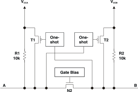
The TXS0101 architecture (see Figure 10) does not require a direction-control signal to control the direction of data flow from A to B or from B to A.
 Figure 10. Architecture of a TXS01xx Cell
Each A-port I/O has an internal 10 kΩ pullup resistor to VCCA, and each B-port I/O has an internal 10 kΩ pullup resistor to VCCB. The output one-shots detect rising edges on the A or B ports. During a rising edge, the one-shot turns on the PMOS transistors (T1,T2) for a short duration, which speeds up the low-to-high transition.
8.3.2 Input Driver Requirements
The fall time (tfA, tfB) of a signal depends on the output impedance of the external device driving the data I/Os of the TXS0101. Similarly, the tPHL and max data rates also depend on the output impedance of the external driver. The values for tfA, tfB, tPHL, and maximum data rates in the data sheet assume that the output impedance of the external driver is less than 50 Ω.
8.3.3 Power Up
During operation, ensure that VCCA ≤ VCCB at all times. During power-up sequencing, VCCA ≥ VCCB does not damage the device, so any power supply can be ramped up first.
8.3.4 Enable and Disable
The TXS0101 has an OE input that is used to disable the device by setting OE low, which places all I/Os in the Hi-Z state. The disable time (tdis) indicates the delay between the time when OE goes low and when the outputs actually get disabled (Hi-Z). The enable time (ten) indicates the amount of time the user must allow for the one-shot circuitry to become operational after OE is taken high.
8.3.5 Pullup or Pulldown Resistors on I/O Lines
Each A-port I/O has an internal 10 kΩ pullup resistor to VCCA, and each B-port I/O has an internal 10 kΩ pullup resistor to VCCB. If a smaller value of pullup resistor is required, an external resistor must be added from the I/O to VCCA or VCCB (in parallel with the internal 10 kΩ resistors).
8.4 Device Functional Modes
The TXS0101 device has two functional modes, enabled and disabled. To disable the device set the OE input low, which places all I/Os in a high impedance state. Setting the OE input high will enable the device.