SCES638D October 2007 – June 2017 TXS0101
PRODUCTION DATA.
- 1 Features
- 2 Applications
- 3 Description
- 4 Revision History
- 5 Pin Configuration and Functions
-
6 Specifications
- 6.1 Absolute Maximum Ratings
- 6.2 ESD Ratings
- 6.3 Recommended Operating Conditions
- 6.4 Thermal Information
- 6.5 Electrical Characteristics
- 6.6 Timing Requirements: V CCA = 1.8 V ± 0.15 V
- 6.7 Timing Requirements VCCA = 2.5 V ± 0.2 V
- 6.8 Timing Requirements: 3.3 V ± 0.3 V
- 6.9 Switching Characteristics: VCCA = 1.8 V ± 0.15 V
- 6.10 Switching Characteristics: VCCA = 2.5 V ± 0.2 V
- 6.11 Switching Characteristics: VCCA = 3.3 V ± 0.3 V
- 6.12 Typical Characteristics
- 7 Parameter Measurement Information
- 8 Detailed Description
- 9 Application and Implementation
- 10Power Supply Recommendations
- 11Layout
- 12Device and Documentation Support
- 13Mechanical, Packaging, and Orderable Information
封装选项
机械数据 (封装 | 引脚)
散热焊盘机械数据 (封装 | 引脚)
订购信息
7 Parameter Measurement Information
7.1 Load Circuits
Figure 4 shows the push-pull driver circuit used for measuring data rate, pulse duration, propagation delay, output rise-time and fall-time. Figure 5 shows the open-drain driver circuit used for measuring data rate, pulse duration, propagation delay, output rise-time and fall-time.
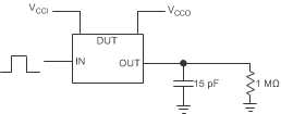 Figure 4. Data Rate, Pulse Duration, Propagation Delay, Output Rise-Time and Fall-Time Measurement Using a Push-Pull Driver
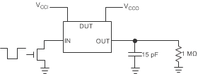 Figure 5. Data Rate, Pulse Duration, Propagation Delay, Output Rise-Time and Fall-Time Measurement Using an Open-Drain Driver
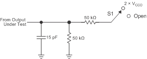 Figure 6. Load Circuit for Enable-Time and Disable-Time Measurement
| TEST | S1 |
|---|---|
| tPZL / tPLZ
(tdis) |
2 × VCCO |
| tPHZ / tPZH
(ten) |
Open |
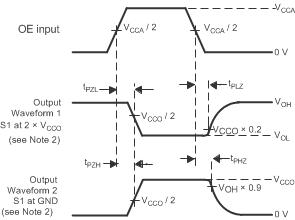
- tPLZ and tPHZ are the same as tdis.
- tPZL and tPZH are the same as ten.
- VCCI is the VCC associated with the input port.
- VCCO is the VCC associated with the output port.
7.2 Voltage Waveforms

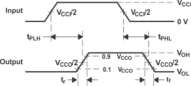 Figure 8. Propagation Delay Times
- CL includes probe and jig capacitance.
- Waveform 1 in Figure 9 is for an output with internal such that the output is high, except when OE is high (see Figure 6). Waveform 2 in Figure 9 is for an output with conditions such that the output is low, except when OE is high.
- All input pulses are supplied by generators having the following characteristics: PRR ≤ 10 MHz, ZO = 50 Ω, dv/dt ≥ 1 V/ns.
- The outputs are measured one at a time, with one transition per measurement.
- tPLZ and tPHZ are the same as tdis.
- tPZL and tPZH are the same as ten.
- tPLH and tPHL are the same as tpd.
- VCCI is the VCC associated with the input port.
- VCCO is the VCC associated with the output port.