ZHCSCI1F November 2013 – October 2024 TXS0104E-Q1
PRODUCTION DATA
- 1
- 1 特性
- 2 应用
- 3 说明
- 4 Pin Configuration and Functions
-
5 Specifications
- 5.1 Absolute Maximum Ratings
- 5.2 ESD Ratings
- 5.3 Recommended Operating Conditions
- 5.4 Thermal Information
- 5.5 Electrical Characteristics
- 5.6 Timing Requirements—VCCA = 1.8 V ± 0.15 V
- 5.7 Timing Requirements—VCCA = 2.5 V ± 0.2 V
- 5.8 Timing Requirements—VCCA = 3.3 V ± 0.3 V
- 5.9 Switching Characteristics—VCCA = 1.8 V ± 0.15 V
- 5.10 Switching Characteristics—VCCA = 2.5 V ± 0.2 V
- 5.11 Switching Characteristics—VCCA = 3.3 V ± 0.3 V
- 5.12 Typical Characteristics
- 6 Parameter Measurement Information
- 7 Detailed Description
- 8 Application and Implementation
- 9 Device and Documentation Support
- 10静电放电警告
- 11术语表
- 12Revision History
- 13Mechanical, Packaging, and Orderable Information
封装选项
请参考 PDF 数据表获取器件具体的封装图。
机械数据 (封装 | 引脚)
- RUT|12
- PW|14
- BQA|14
散热焊盘机械数据 (封装 | 引脚)
- BQA|14
订购信息
6.1 Load Circuits
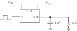
 Figure 6-1 Data Rate, Pulse Duration, Propagation Delay, Output Rise-Time and Fall-Time Measurement Using a Push-Pull Driver
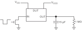
 Figure 6-2 Data Rate, Pulse Duration, Propagation Delay, Output Rise-Time and Fall-Time Measurement Using an Open-Drain Driver
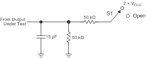
| TEST | S1 | ||
| tPZL / tPLZ (tdis) | 2 × VCCO | ||
| tPHZ / tPZH (ten) | Open | ||
- tPLZ and tPHZ are the same as tdis.
- tPZL and tPZH are the same as ten.
- VCCI is the VCC associated with the input port.
- VCCO is the VCC associated with the output port.