ZHCSCI1F November 2013 – October 2024 TXS0104E-Q1
PRODUCTION DATA
- 1
- 1 特性
- 2 应用
- 3 说明
- 4 Pin Configuration and Functions
-
5 Specifications
- 5.1 Absolute Maximum Ratings
- 5.2 ESD Ratings
- 5.3 Recommended Operating Conditions
- 5.4 Thermal Information
- 5.5 Electrical Characteristics
- 5.6 Timing Requirements—VCCA = 1.8 V ± 0.15 V
- 5.7 Timing Requirements—VCCA = 2.5 V ± 0.2 V
- 5.8 Timing Requirements—VCCA = 3.3 V ± 0.3 V
- 5.9 Switching Characteristics—VCCA = 1.8 V ± 0.15 V
- 5.10 Switching Characteristics—VCCA = 2.5 V ± 0.2 V
- 5.11 Switching Characteristics—VCCA = 3.3 V ± 0.3 V
- 5.12 Typical Characteristics
- 6 Parameter Measurement Information
- 7 Detailed Description
- 8 Application and Implementation
- 9 Device and Documentation Support
- 10静电放电警告
- 11术语表
- 12Revision History
- 13Mechanical, Packaging, and Orderable Information
封装选项
请参考 PDF 数据表获取器件具体的封装图。
机械数据 (封装 | 引脚)
- RUT|12
- PW|14
- BQA|14
散热焊盘机械数据 (封装 | 引脚)
- BQA|14
订购信息
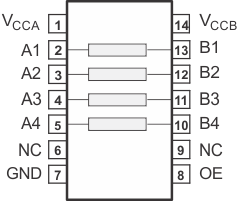
4 Pin Configuration and Functions

NC - No
internal connection
Figure 4-1 PW Package,14-Pin TSSOP(Top View)
NC - No
internal connection
Figure 4-2 BQA Package,14-Pin WQFN(Top View)Table 4-1 Pin Functions
| PIN | TYPE(1) | DESCRIPTION | |
|---|---|---|---|
| NAME | NO. | ||
| A1 | 2 | I/O | Input-output 1 for the A port. This pin is referenced to VCCA. |
| A2 | 3 | I/O | Input-output 2 for the A port. This pin is referenced to VCCA. |
| A3 | 4 | I/O | Input-output 3 for the A port. This pin is referenced to VCCA. |
| A4 | 5 | I/O | Input-output 4 for the A port. This pin is referenced to VCCA. |
| B1 | 13 | I/O | Input-output 1 for the B port. This pin is referenced to VCCB. |
| B2 | 12 | I/O | Input-output 2 for the B port. This pin is referenced to VCCB. |
| B3 | 11 | I/O | Input-output 3 for the B port. This pin is referenced to VCCB. |
| B4 | 10 | I/O | Input-output 4 for the B port. This pin is referenced to VCCB. |
| GND | 7 | — | Ground |
| NC | 6 | — | No connection |
| 9 | |||
| OE | 8 | I | Tri-state output-mode enable. Pull the OE pin low to place all outputs in tri-state mode. This pin is referenced to VCCA. |
| VCCA | 1 | I | A-port supply voltage. 1.65 V ≤ VCCA ≤ 3.6 V and VCCA ≤ VCCB. |
| VCCB | 14 | I | B-port supply voltage. 2.3 V ≤ VCCB ≤ 5.5 V. |
(1) I = input, O = output
 Figure 4-3 RUT Package, 12-Pin UQFN
(Transparent Top View)
Figure 4-3 RUT Package, 12-Pin UQFN
(Transparent Top View)Table 4-2 Pin Functions: RUT
| PIN | TYPE(1) | DESCRIPTION | |
|---|---|---|---|
| NAME | NO. | ||
| A1 | 2 | I/O | Input/output A1. Referenced to VCCA. |
| A2 | 3 | I/O | Input/output A2. Referenced to VCCA. |
| A3 | 4 | I/O | Input/output A3. Referenced to VCCA. |
| A4 | 5 | I/O | Input/output A4. Referenced to VCCA. |
| B1 | 10 | I/O | Input/output B1. Referenced to VCCB. |
| B2 | 9 | I/O | Input/output B2. Referenced to VCCB. |
| B3 | 8 | I/O | Input/output B3. Referenced to VCCB. |
| B4 | 7 | I/O | Input/output B4. Referenced to VCCB. |
| GND | 6 | — | Ground |
| OE | 12 | I | 3-state output-mode enable. Pull OE low to place all outputs in 3-state mode. Referenced to VCCA. |
| VCCA | 1 | — | A-port supply voltage. 1.65 V ≤ VCCA ≤ 3.6 V and VCCA ≤ VCCB. |
| VCCB | 11 | — | A-port supply voltage. 1.65 V ≤ VCCA ≤ 3.6 V and VCCA ≤ VCCB. |
(1) I = input, O = output