ZHCS910B November 2011 – April 2016 TXS0206A
PRODUCTION DATA.
- 1 特性
- 2 应用范围
- 3 说明
- 4 修订历史记录
- 5 Pin Configuration and Functions
-
6 Specifications
- 6.1 Absolute Maximum Ratings
- 6.2 ESD Ratings
- 6.3 Recommended Operating Conditions
- 6.4 Thermal Information
- 6.5 Electrical Characteristics
- 6.6 Timing Requirements—VCCA = 1.2 V ± 0.1 V
- 6.7 Timing Requirements—VCCA = 1.8 V ± 0.15 V
- 6.8 Timing Requirements—VCCA = 3.3 V ± 0.3 V
- 6.9 Switching Characteristics—VCCA = 1.2 V ± 0.1 V
- 6.10 Switching Characteristics—VCCA = 1.8 V ± 0.15 V
- 6.11 Switching Characteristics—VCCA = 3.3 V ± 0.3 V
- 6.12 Operating Characteristics —VCCA = 1.2 V
- 6.13 Operating Characteristics —VCCA = 1.8 V
- 6.14 Operating Characteristics — VCCA = 3.3 V
- 6.15 Typical Characteristics
- 7 Parameter Measurement Information
- 8 Detailed Description
- 9 Application and Implementation
- 10Power Supply Recommendations
- 11Layout
- 12器件和文档支持
- 13机械、封装和可订购信息
11 Layout
11.1 Layout Guidelines
To ensure reliability of the device, TI recommends following common printed-circuit board layout guidelines.
- Bypass capacitors should be used on power supplies.
- Short trace lengths should be used to avoid excessive loading
- PCB signal trace-lengths must be kept short enough so that the round-trip delay of any reflection is less than the one shot duration, approximately 30 ns, ensuring that any reflection encounters low impedance at the source driver
- With very heavy capacitive loads, the one-shot can time-out before the signal is driven fully to the positive rail, so it is recommended that this lumped-load capacitance be considered and kept below 50 pF to avoid O.S. retriggering, bus contention, output signal oscillations, or other adverse system-level affects.
11.2 Layout Example
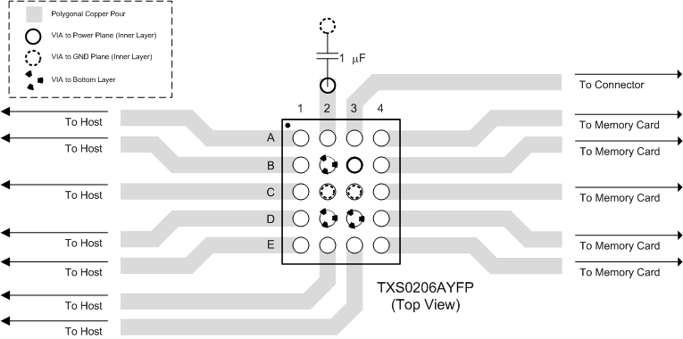
 Figure 10. TXS0206A Example Layout (Top Layer)
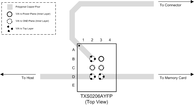
 Figure 11. TXS0206A Example Layout (Bottom Layer)