ZHCSPL2 August 2022 TXU0102-Q1
PRODUCTION DATA
- 1 特性
- 2 应用
- 3 说明
- 4 Revision History
- 5 Pin Configuration and Functions—TXU0102-Q1
-
6 Specifications
- 6.1 Absolute Maximum Ratings
- 6.2 ESD Ratings
- 6.3 Recommended Operating Conditions
- 6.4 Thermal Information
- 6.5 Electrical Characteristics
- 6.6 Switching Characteristics, VCCA = 1.2 ± 0.1 V
- 6.7 Switching Characteristics, VCCA = 1.5 ± 0.1 V
- 6.8 Switching Characteristics, VCCA = 1.8 ± 0.15 V
- 6.9 Switching Characteristics, VCCA = 2.5 ± 0.2 V
- 6.10 Switching Characteristics, VCCA = 3.3 ± 0.3 V
- 6.11 Switching Characteristics, VCCA = 5.0 ± 0.5 V
- 6.12 Operating Characteristics
- 6.13 Typical Characteristics
- 7 Parameter Measurement Information
-
8 Detailed Description
- 8.1 Overview
- 8.2 Functional Block Diagram
- 8.3
Feature Description
- 8.3.1 CMOS Schmitt-Trigger Inputs with Integrated Pulldowns
- 8.3.2 Control Logic (OE) with VCC(MIN) Circuitry
- 8.3.3 Balanced High-Drive CMOS Push-Pull Outputs
- 8.3.4 VCC Isolation and VCC Disconnect
- 8.3.5 Over-Voltage Tolerant Inputs
- 8.3.6 Glitch-Free Power Supply Sequencing
- 8.3.7 Negative Clamping Diodes
- 8.3.8 Fully Configurable Dual-Rail Design
- 8.3.9 Supports High-Speed Translation
- 8.4 Device Functional Modes
- 9 Application and Implementation
- 10Power Supply Recommendations
- 11Layout
- 12Device and Documentation Support
- 13Mechanical, Packaging, and Orderable Information
7.1 Load Circuit and Voltage Waveforms
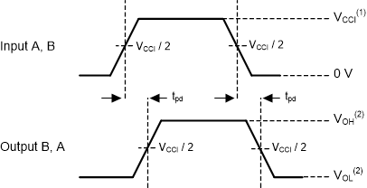
Unless otherwise noted, generators supply all input pulses that have the following characteristics:
- f = 1 MHz
- ZO = 50 Ω
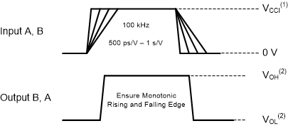
- Δt/ΔV ≤ 1 ns/V

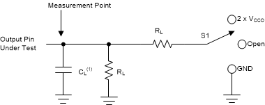
- CL includes probe and jig capacitance.
Table 7-1 Load Circuit
Conditions
| Parameter | VCCO | RL | CL | S1 | VTP | |
|---|---|---|---|---|---|---|
| tpd | Propagation (delay) time | 1.1 V – 5.5 V | 10 kΩ | 5 pF | Open | N/A |
| ten, tdis | Enable time, disable time | 1.1 V – 1.6 V | 10 kΩ | 5 pF | 2 × VCCO | 0.1 V |
| 1.65 V – 2.7 V | 10 kΩ | 5 pF | 2 × VCCO | 0.15 V | ||
| 3.0 V – 5.5 V | 10 kΩ | 5 pF | 2 × VCCO | 0.3 V | ||
| ten, tdis | Enable time, disable time | 1.1 V – 1.6 V | 10 kΩ | 5 pF | GND | 0.1 V |
| 1.65 V – 2.7 V | 10 kΩ | 5 pF | GND | 0.15 V | ||
| 3.0 V – 5.5 V | 10 kΩ | 5 pF | GND | 0.3 V | ||

- VCCI is the supply pin associated with the input port.
- VOH and VOL are typical output voltage levels that occur with specified RL, CL, and S1

- VCCI is the supply pin associated with the input port.
- VOH and VOL are typical output voltage levels that occur with specified RL, CL, and S1

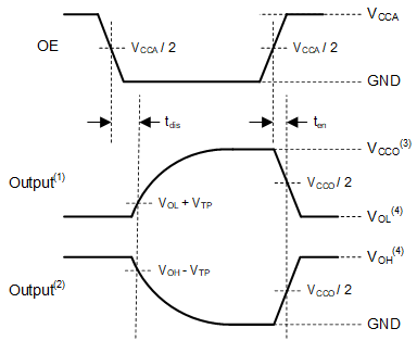
- Output waveform on the condition that input is driven to a valid Logic Low.
- Output waveform on the condition that input is driven to a valid Logic High.
- VCCO is the supply pin associated with the output port.
- VOH and VOL are typical output voltage levels with specified RL, CL, and S1.