ZHCSPL2 August 2022 TXU0102-Q1
PRODUCTION DATA
- 1 特性
- 2 应用
- 3 说明
- 4 Revision History
- 5 Pin Configuration and Functions—TXU0102-Q1
-
6 Specifications
- 6.1 Absolute Maximum Ratings
- 6.2 ESD Ratings
- 6.3 Recommended Operating Conditions
- 6.4 Thermal Information
- 6.5 Electrical Characteristics
- 6.6 Switching Characteristics, VCCA = 1.2 ± 0.1 V
- 6.7 Switching Characteristics, VCCA = 1.5 ± 0.1 V
- 6.8 Switching Characteristics, VCCA = 1.8 ± 0.15 V
- 6.9 Switching Characteristics, VCCA = 2.5 ± 0.2 V
- 6.10 Switching Characteristics, VCCA = 3.3 ± 0.3 V
- 6.11 Switching Characteristics, VCCA = 5.0 ± 0.5 V
- 6.12 Operating Characteristics
- 6.13 Typical Characteristics
- 7 Parameter Measurement Information
-
8 Detailed Description
- 8.1 Overview
- 8.2 Functional Block Diagram
- 8.3
Feature Description
- 8.3.1 CMOS Schmitt-Trigger Inputs with Integrated Pulldowns
- 8.3.2 Control Logic (OE) with VCC(MIN) Circuitry
- 8.3.3 Balanced High-Drive CMOS Push-Pull Outputs
- 8.3.4 VCC Isolation and VCC Disconnect
- 8.3.5 Over-Voltage Tolerant Inputs
- 8.3.6 Glitch-Free Power Supply Sequencing
- 8.3.7 Negative Clamping Diodes
- 8.3.8 Fully Configurable Dual-Rail Design
- 8.3.9 Supports High-Speed Translation
- 8.4 Device Functional Modes
- 9 Application and Implementation
- 10Power Supply Recommendations
- 11Layout
- 12Device and Documentation Support
- 13Mechanical, Packaging, and Orderable Information
6.13 Typical Characteristics
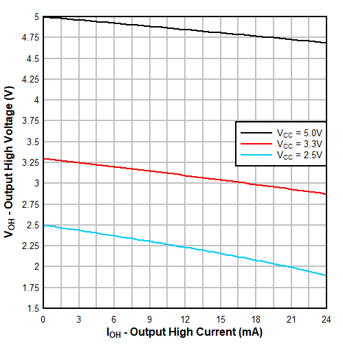 Figure 6-1 Typical
(TA=25°C) Output High Voltage (VOH) vs Source Current
(IOH)
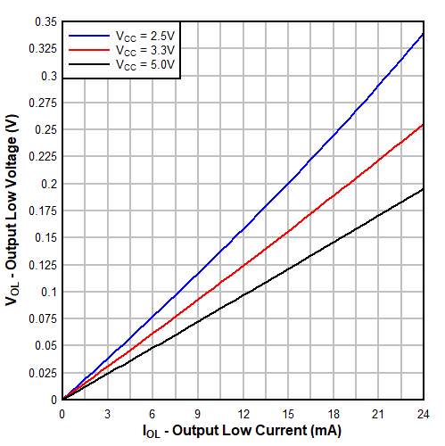 Figure 6-3 Typical
(TA=25°C) Output Low Voltage (VOL) vs Sink Current
(IOL)
 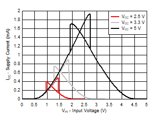 Figure 6-5 Typical
(TA=25°C) Supply Current (ICC) vs Input Voltage
(VIN)
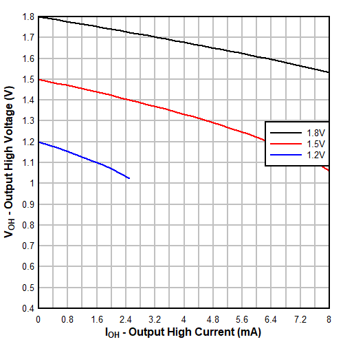 Figure 6-2 Typical
(TA=25°C) Output High Voltage (VOH) vs Source Current
(IOH)
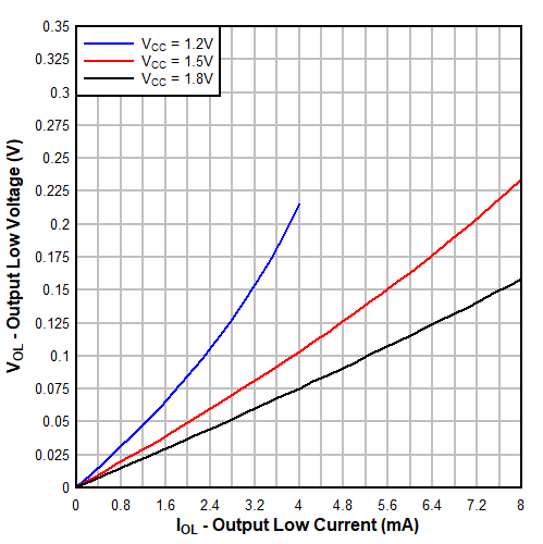 Figure 6-4 Typical
(TA=25°C) Output Low Voltage (VOL) vs Sink Current
(IOL)
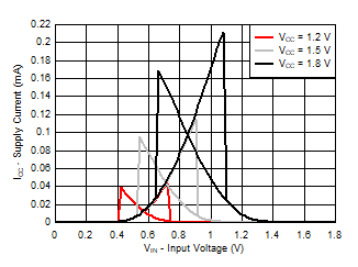 Figure 6-6 Typical
(TA=25°C) Supply Current (ICC) vs Input Voltage
(VIN)