ZHCSHE5G November 1970 – January 2018
PRODUCTION DATA.
- 1 特性
- 2 应用
- 3 说明
- 4 修订历史记录
- 5 Pin Configurations and Functions
- 6 Specifications
- 7 Detailed Description
- 8 Application and Implementation
- 9 Power Supply Recommendations
- 10Layout
- 11器件和文档支持
- 12机械、封装和可订购信息
封装选项
机械数据 (封装 | 引脚)
散热焊盘机械数据 (封装 | 引脚)
- PS|8
订购信息
8.1 Application Information
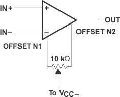
The input offset voltage of operational amplifiers (op amps) arises from unavoidable mismatches in the differential input stage of the op-amp circuit caused by mismatched transistor pairs, collector currents, current-gain betas (β), collector or emitter resistors and so forth. The input offset pins allow the designer to adjust for mismatches resulting from external circuitry. These input mismatches can be adjusted by placing resistors or a potentiometer between the inputs as shown in Figure 12. A potentiometer can fine-tune the circuit during testing or for applications which require precision offset control. For more information about designing using the input-offset pins, see Nulling Input Offset Voltage of Operational Amplifiers.
 Figure 12. Input Offset Voltage Null Circuit