ZHCSMC3X january 1976 – june 2023 UA78L
PRODUCTION DATA
- 1
- 1 特性
- 2 应用
- 3 说明
- 4 Revision History
- 5 Pin Configuration and Functions
-
6 Specifications
- 6.1 Absolute Maximum Ratings
- 6.2 ESD Ratings
- 6.3 Recommended Operating Conditions
- 6.4 Thermal Information
- 6.5 Electrical Characteristics: UA78L02 (Legacy Chip Only)
- 6.6 Electrical Characteristics: UA78L033 (New Chip Only)
- 6.7 Electrical Characteristics: UA78L05 (Both Legacy and New Chip)
- 6.8 Electrical Characteristics: UA78L12 (Both Legacy and New Chip)
- 6.9 Electrical Characteristics: UA78L06 (Legacy Chip Only)
- 6.10 Electrical Characteristics: UA78L08 (Legacy Chip Only)
- 6.11 Electrical Characteristics: UA78L09 (Legacy Chip Only)
- 6.12 Electrical Characteristics: UA78L10 (Legacy Chip Only)
- 6.13 Electrical Characteristics: UA78L15 (Both Legacy and New Chip)
- 6.14 Typical Characteristics
- 7 Detailed Description
- 8 Applications and Implementation
- 9 Device and Documentation Support
- 10Mechanical, Packaging, and Orderable Information
封装选项
请参考 PDF 数据表获取器件具体的封装图。
机械数据 (封装 | 引脚)
- D|8
- PK|3
- LP|3
散热焊盘机械数据 (封装 | 引脚)
- PK|3
订购信息
5 Pin Configuration and Functions
 Figure 5-1 D Package,8-Pin SOIC(Top View)
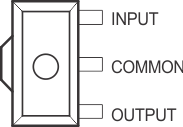
 Figure 5-3 PK Package,3-Pin SOT-89(Top View)
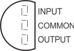
 Figure 5-2 LP Package,3-Pin TO-92(Top View)
| PIN | TYPE | DESCRIPTION | |||
|---|---|---|---|---|---|
| NAME | SOIC | TO-92 | SOT-89 | ||
| COMMON | 2, 3, 6, 7 | 2 | 2 | — | Ground |
| INPUT | 8 | 3 | 3 | I | Input pin. Use the recommended capacitor value as listed in the Recommended Operating Conditions table. Place the input capacitor as close to the IN and GND pins of the device as possible. |
| OUTPUT | 1 | 1 | 1 | O | Output pin. Use the recommended capacitor value as listed in the Recommended Operating Conditions table. Place the output capacitor as close to the OUT and GND pins of the device as possible. |
| NC | 4, 5 | — | — | — | No connect pin. This pin is not connected internally. Connect this pin to ground for best thermal performance or leave floating. |