ZHCSJJ9A april   2019  – december 2020 UC1825B-SP

PRODUCTION DATA  

  1.   1
  2. 特性
  3. 应用
  4. 说明
  5. Revision History
  6. Pin Configuration and Functions
  7. Specifications
    1. 6.1 Absolute Maximum Ratings
    2. 6.2 ESD Ratings
    3. 6.3 Recommended Operating Conditions
    4. 6.4 Thermal Information
    5. 6.5 Electrical Characteristics
    6. 6.6 Typical Characteristics
  8. Detailed Description
    1. 7.1 Overview
    2. 7.2 Functional Block Diagram
    3. 7.3 Feature Description
      1. 7.3.1 Control Methods
      2. 7.3.2 Synchronization
      3. 7.3.3 High Current Outputs
      4. 7.3.4 Open Loop Test Circuit
    4. 7.4 Device Functional Modes
  9. Application and Implementation
    1. 8.1 Application Information
    2. 8.2 Typical Application
      1. 8.2.1 System Design Theory
        1. 8.2.1.1 Switching Frequency
        2. 8.2.1.2 Transformer
        3. 8.2.1.3 RCD and Diode Clamp
        4. 8.2.1.4 Output Diode
        5. 8.2.1.5 Main Switching MOSFETs
        6. 8.2.1.6 Output Filter and Capacitance
        7. 8.2.1.7 Compensation
        8. 8.2.1.8 Sense Resistor
    3. 8.3 Application Curves
  10. Power Supply Recommendations
  11. 10Layout
    1. 10.1 Layout Guidelines
      1. 10.1.1 Feedback Traces
      2. 10.1.2 Input/Output Capacitors
      3. 10.1.3 Compensation Components
      4. 10.1.4 Traces and Ground Planes
      5. 10.1.5 Ground Planes
    2. 10.2 Layout Example
  12. 11Device and Documentation Support
    1. 11.1 Documentation Support
      1. 11.1.1 Related Documentation
    2. 11.2 接收文档更新通知
    3. 11.3 支持资源
    4. 11.4 Trademarks
    5. 11.5 静电放电警告
    6. 11.6 术语表
  13. 12Mechanical, Packaging, and Orderable Information

封装选项

机械数据 (封装 | 引脚)
散热焊盘机械数据 (封装 | 引脚)
订购信息

Application Curves

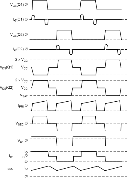
GUID-CB1C6316-0886-4EB6-AA5C-C2298F6CA00F-low.gifFigure 8-5 Basic Push-Pull Waveforms
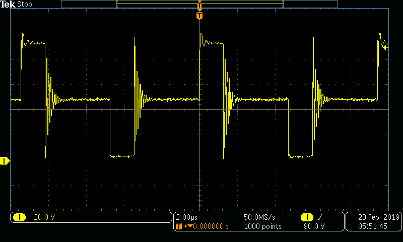
GUID-3CBA4A90-E2F4-4D93-BF98-CA802EF87C5D-low.pngFigure 8-6 Voltage Stress Across Main Switching MOSFETS Q1 and Q2

The test in Figure 8-6 was done with 48-V input and a 10-A output load.
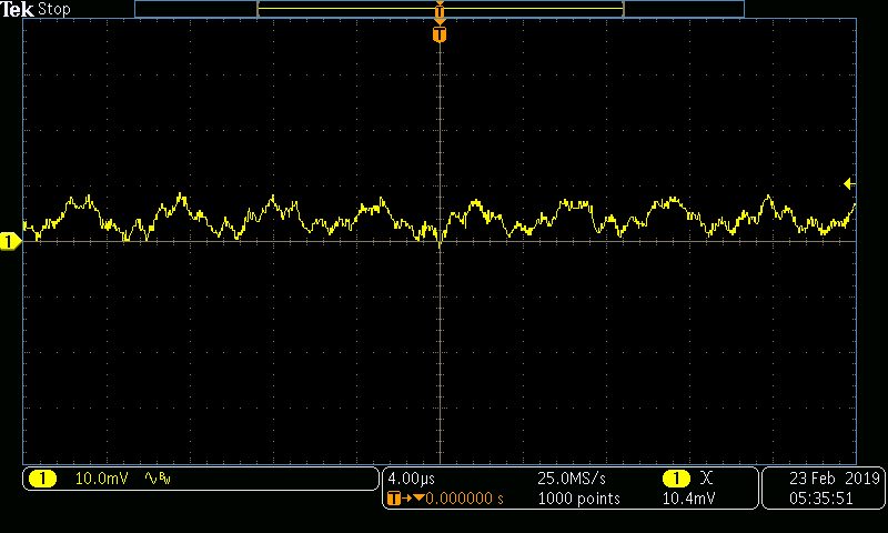
GUID-027D7E19-1278-4685-AC69-14F7DB97D985-low.pngFigure 8-7 Output Voltage Ripple With 48 VIN

Output voltage ripple test in Figure 8-7 was done with 48-V input and 10-A output current.
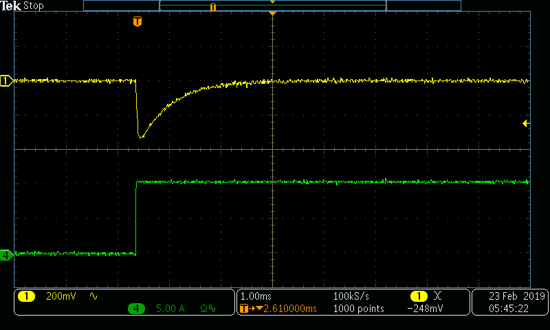
GUID-19939B1A-DDA8-4A81-ACC6-BC3A15D54FD2-low.pngFigure 8-8 Full Output Voltage Transient With 48 VIN

Full step up transient in Figure 8-8 was done with 48-V input and output current was stepped from 0 A to 10 A.