ZHCSDP1E January   2009  – February 2019 UC1842A-SP , UC1844A-SP

PRODUCTION DATA.  

  1. 特性
  2. 应用
  3. 说明
    1.     Device Images
      1.      简化原理图
  4. 修订历史记录
  5. Device Comparison Table
  6. Pin Configuration and Functions
    1.     Pin Functions
  7. Specifications
    1. 7.1 Absolute Maximum Ratings
    2. 7.2 ESD Ratings
    3. 7.3 Recommended Operating Conditions
    4. 7.4 Thermal Information
    5. 7.5 Electrical Characteristics
    6. 7.6 Electrical Characteristics (Radiation-Improved Devices)
    7. 7.7 Typical Characteristics
  8. Detailed Description
    1. 8.1 Overview
    2. 8.2 Functional Block Diagram
    3. 8.3 Feature Description
      1. 8.3.1 UVLO
      2. 8.3.2 Reference
      3. 8.3.3 Totem-Pole Output
    4. 8.4 Device Functional Modes
  9. Application and Implementation
    1. 9.1 Application Information
    2. 9.2 Typical Application
      1. 9.2.1 Design Requirements
      2. 9.2.2 Detailed Design Procedure
        1. 9.2.2.1 Oscillator
        2. 9.2.2.2 Current Sensing and Limiting
        3. 9.2.2.3 Error Amplifier
      3. 9.2.3 Application Curves
  10. 10Power Supply Recommendations
  11. 11Layout
    1. 11.1 Layout Guidelines
      1. 11.1.1 Feedback Traces
      2. 11.1.2 Input/Output Capacitors
      3. 11.1.3 Compensation Components
      4. 11.1.4 Traces and Ground Planes
    2. 11.2 Layout Example
  12. 12器件和文档支持
    1. 12.1 相关链接
    2. 12.2 接收文档更新通知
    3. 12.3 社区资源
    4. 12.4 商标
    5. 12.5 静电放电警告
    6. 12.6 术语表
  13. 13机械、封装和可订购信息

封装选项

机械数据 (封装 | 引脚)
散热焊盘机械数据 (封装 | 引脚)
订购信息

Oscillator

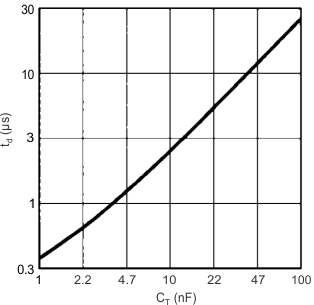
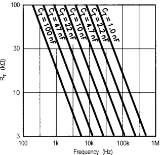
The UC184xA-SP oscillator is programmed as shown in Figure 15. Timing capacitor CT is charged from VREF (5 V) through the timing resistor RT, and discharged by an internal current source. The first step in selecting the oscillator components is to determine the required circuit dead time. Once obtained, Figure 16 is used to pinpoint the nearest standard value of CT for a given dead time. Next, the appropriate RT value is interpolated using the parameters for CT and oscillator frequency. Figure 17 shows the RT/CT combinations versus oscillator frequency. The timing resistor can be calculated from the following formula.

Equation 1. UC1842A-SP UC1844A-SP eqn1_slusci6.gif
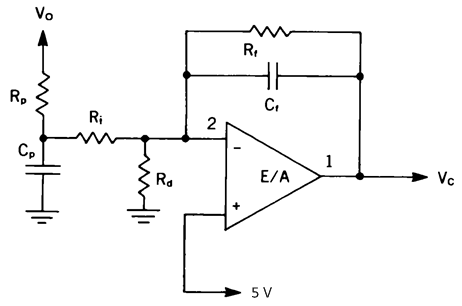
UC1842A-SP UC1844A-SP sch_EA_comp_LUSC14.gifFigure 14. E/A Compensation Circuit for Continuous Boost and Flyback Topologies

The UC184xA-SP has an internal divide-by-two flip-flop driven by the oscillator for a 50% maximum duty cycle. Therefore, their oscillators must be set to run at twice the desired power supply switching frequency.
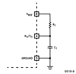
UC1842A-SP UC1844A-SP oscillator_LUSC14.gifFigure 15. Oscillator Programming
UC1842A-SP UC1844A-SP gr_dt_vs_Ct_lusc14.gifFigure 16. Dead Time vs CT (RT > 5 kΩ)
UC1842A-SP UC1844A-SP gr_RT_freq_lusc14.gifFigure 17. Timing Resistance vs Frequency