ZHCSJK0A April   2019  – September 2019 UC1843B-SP

PRODUCTION DATA.  

  1. 特性
  2. 应用
  3. 说明
    1.     Device Images
      1.      简化原理图
  4. 修订历史记录
  5. Pin Configuration and Functions
    1.     Pin Functions
  6. Specifications
    1. 6.1 Absolute Maximum Ratings
    2. 6.2 ESD Ratings
    3. 6.3 Recommended Operating Conditions
    4. 6.4 Thermal Information
    5. 6.5 Electrical Characteristics
    6. 6.6 Typical Characteristics
  7. Detailed Description
    1. 7.1 Overview
    2. 7.2 Functional Block Diagram
    3. 7.3 Feature Description
      1. 7.3.1 UVLO
      2. 7.3.2 Reference
      3. 7.3.3 Totem-Pole Output
    4. 7.4 Device Functional Modes
  8. Application and Implementation
    1. 8.1 Application Information
    2. 8.2 Typical Application
      1. 8.2.1 Design Requirements
      2. 8.2.2 Detailed Design Procedure
        1. 8.2.2.1 Switching Frequency
        2. 8.2.2.2 Transformer
        3. 8.2.2.3 RCD Diode Clamp
        4. 8.2.2.4 Output Diode
        5. 8.2.2.5 Output Filter and Capacitor
        6. 8.2.2.6 Compensation
        7. 8.2.2.7 Sense Resistor and Slope Compensation
      3. 8.2.3 Application Curves
  9. Power Supply Recommendations
  10. 10Layout
    1. 10.1 Layout Guidelines
      1. 10.1.1 Feedback Traces
      2. 10.1.2 Input/Output Capacitors
      3. 10.1.3 Compensation Components
      4. 10.1.4 Traces and Ground Planes
    2. 10.2 Layout Example
  11. 11器件和文档支持
    1. 11.1 接收文档更新通知
    2. 11.2 社区资源
    3. 11.3 商标
    4. 11.4 静电放电警告
    5. 11.5 Glossary
  12. 12机械、封装和可订购信息

封装选项

机械数据 (封装 | 引脚)
散热焊盘机械数据 (封装 | 引脚)
订购信息

Application Curves

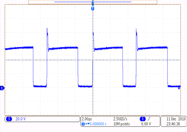
UC1843B-SP tida-070002-waveform-21-switch-node.pngFigure 12. Switch Node of Flyback Converter

For the test in Figure 12, 40 V was applied to the input and 10 A was drawn from the output. Ringing can be present on the switching node if the converter is run in discontinuous conduction mode rather than the continuous conduction mode the design was run with.
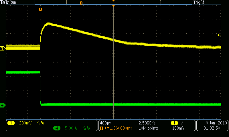
UC1843B-SP SLHR016_40V_Down_Step.pngFigure 13. Load Step Down With 40 VIN
UC1843B-SP SLHR016_40V_Up_Step.pngFigure 14. Load Step Up With 40 VIN

For tests shown in and , 40 V was applied to the input and a load step was applied to the output. The load step applied was from 0 A to 10 A and 10 A to 0 A. Note that those currents do not include the 0.1-A pre-load. The curves show that the stability of the design due to the lack of ringing during the load step.