ZHCSDP1E January 2009 – February 2019 UC1842A-SP , UC1844A-SP
PRODUCTION DATA.
8.3.3 Totem-Pole Output
The UC184xA-SP PWM has a single totem-pole output which can be operated to ±1-A peak for driving MOSFET gates, and a +200 mA average current for bipolar power U-100A transistors. Cross conduction between the output transistors is minimal, the average added power with VIN = 30 V is only 80 mW at 200 kHz.
Limiting the peak current through the IC is accomplished by placing a resistor between the totem-pole output and the gate of the MOSFET. The value is determined by dividing the totem-pole collector voltage VC by the peak current rating of the IC’s totem-pole. Without this resistor, the peak current is limited only by the dV/dT rate of the totem-pole switching and the FET gate capacitance.
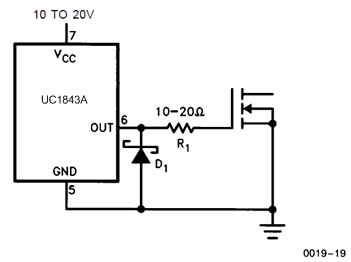
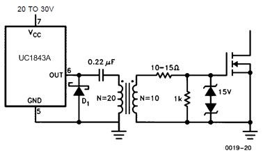
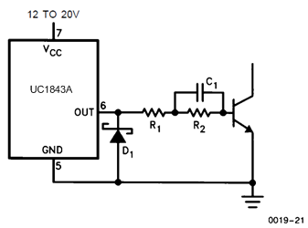
The use of a Schottky diode from the PWM output to ground prevents the output voltage from going excessively below ground, causing instabilities within the IC. To be effective, the diode selected should have a forward drop of less than 0.3 V at 200 mA. Most 1- to 3-A Schottky diodes exhibit these traits above room temperature. Placing the diode as physically close to the PWM as possible enhances circuit performance. Implementation of the complete drive scheme is shown in Figure 8 through Figure 10. Transformer-driven circuits also require the use of the Schottky diodes to prevent a similar set of circumstances from occurring on the PWM output. The ringing below ground is greatly enhanced by the transformer leakage inductance and parasitic capacitance, in addition to the magnetizing inductance and FET gate capacitance. Circuit implementation is similar to the previous example.
Figure 8 through Figure 10 show suggested circuits for driving MOSFETs and bipolar transistors with the UC184xA-SP output. The simple circuit of Figure 8 can be used when the control IC is not electrically isolated from the MOSFET turnon and turnoff to ±1 A. It also provides damping for a parasitic tank circuit formed by the FET input capacitance and series wiring inductance. Schottky diode, D1, prevents the output of the IC from going far below ground during turnoff.
Figure 9 shows an isolated MOSFET drive circuit which is appropriate when the drive signal must be level shifted or transmitted across an isolation boundary. Bipolar transistors can be driven efficiently with the circuit of Figure 10. Resistors R1 and R2 fix the on-state base current while capacitor Cl provides a negative base current pulse to remove stored charge at turnoff.
Because the UC184xA-SP series has only a single output, an interface circuit is needed to control push-pull, half-bridge, or full-bridge topologies. The UC1706 dual output driver with internal toggle flip-flop performs this function. Typical Application shows a typical application for these two ICs. Increased drive capability for driving numerous FETs in parallel, or other loads can be accomplished using one of the UC1705/6/7 driver ICs.
 Figure 8. Direct MOSFET Drive
  Figure 9. Isolated MOSFET Drive
  Figure 10. Bipolar Drive With Negative turnoff Bias