ZHCSDP1E January   2009  – February 2019 UC1842A-SP , UC1844A-SP

PRODUCTION DATA.  

  1. 特性
  2. 应用
  3. 说明
    1.     Device Images
      1.      简化原理图
  4. 修订历史记录
  5. Device Comparison Table
  6. Pin Configuration and Functions
    1.     Pin Functions
  7. Specifications
    1. 7.1 Absolute Maximum Ratings
    2. 7.2 ESD Ratings
    3. 7.3 Recommended Operating Conditions
    4. 7.4 Thermal Information
    5. 7.5 Electrical Characteristics
    6. 7.6 Electrical Characteristics (Radiation-Improved Devices)
    7. 7.7 Typical Characteristics
  8. Detailed Description
    1. 8.1 Overview
    2. 8.2 Functional Block Diagram
    3. 8.3 Feature Description
      1. 8.3.1 UVLO
      2. 8.3.2 Reference
      3. 8.3.3 Totem-Pole Output
    4. 8.4 Device Functional Modes
  9. Application and Implementation
    1. 9.1 Application Information
    2. 9.2 Typical Application
      1. 9.2.1 Design Requirements
      2. 9.2.2 Detailed Design Procedure
        1. 9.2.2.1 Oscillator
        2. 9.2.2.2 Current Sensing and Limiting
        3. 9.2.2.3 Error Amplifier
      3. 9.2.3 Application Curves
  10. 10Power Supply Recommendations
  11. 11Layout
    1. 11.1 Layout Guidelines
      1. 11.1.1 Feedback Traces
      2. 11.1.2 Input/Output Capacitors
      3. 11.1.3 Compensation Components
      4. 11.1.4 Traces and Ground Planes
    2. 11.2 Layout Example
  12. 12器件和文档支持
    1. 12.1 相关链接
    2. 12.2 接收文档更新通知
    3. 12.3 社区资源
    4. 12.4 商标
    5. 12.5 静电放电警告
    6. 12.6 术语表
  13. 13机械、封装和可订购信息

封装选项

机械数据 (封装 | 引脚)
散热焊盘机械数据 (封装 | 引脚)
订购信息

Detailed Design Procedure

See Table 2 for component values.

Table 2. Components(1)

COMPONENT VALUE
R1 5 Ω, 1 W
R2 56 kΩ, 2 W
R3 20 kΩ
R4 4.7 kΩ
R5 150 kΩ
R6 10 kΩ
R7 22 Ω
R8 1 kΩ
R9 68 Ω
R10 0.55 Ω, 1 W
R11 2.7 kΩ, 2 W
R12 4.7 kΩ, 2 W
R13 20 kΩ
C1 250 µF, 250 V
C2 100 µF, 25 V
C3 22 µF
C4 47 µF, 25 V
C5 0.1 µF
C6 0.0022 µF
C7 470 pF
C8 680 pF, 600 V
C9 3300 pF, 600 V
C10 4700 µF, 10 V
C11 4700 µF, 10 V
C12 2200 µF, 10 V
C13 2200 µF, 10 V
C14 100 pF
D2 1N3612
D3 1N3612
D4 1N3613
D5 1N3613
D6 USD945
D7 UFS1002
D8 UES1002
Q1 UFN833
See Figure 11 for reference.
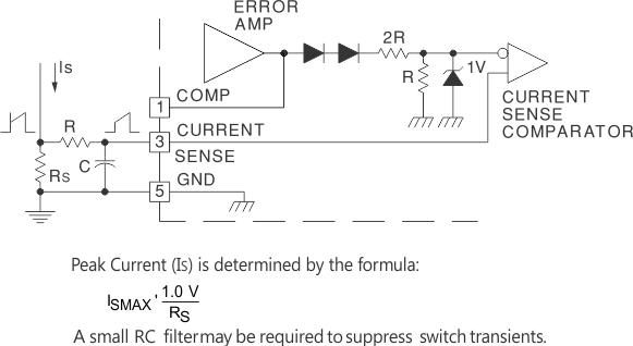
UC1842A-SP UC1844A-SP curr_sense_cx_lus872.gifFigure 12. Current-Sense Circuit
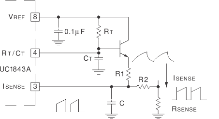
UC1842A-SP UC1844A-SP slope_compensation_lus872.gif

NOTE:

A fraction of the oscillator ramp can be resistively summed with the current sense signal to provide slope compensation for converters requiring duty cycles over 50%.
Capacitor, C, forms a filter with R2 to suppress the leading edge switch spikes.
Figure 13. Slope Compensation