SLUS191D February 1997 – July 2017 UC1525A , UC1527A , UC2525A , UC2527A , UC3525A , UC3527A
PRODUCTION DATA.
- 1 Features
- 2 Applications
- 3 Description
- 4 Revision History
- 5 Pin Configuration and Functions
- 6 Specifications
- 7 Detailed Description
- 8 Application and Implementation
- 9 Power Supply Recommendations
- 10Layout
- 11Device and Documentation Support
- 12Mechanical, Packaging, and Orderable Information
封装选项
请参考 PDF 数据表获取器件具体的封装图。
机械数据 (封装 | 引脚)
- DW|16
- N|16
散热焊盘机械数据 (封装 | 引脚)
订购信息
6 Specifications
6.1 Absolute Maximum Ratings
over operating free-air temperature range (unless otherwise noted)(1)| MIN | MAX | UNIT | ||
|---|---|---|---|---|
| +VIN | Supply voltage | 40 | V | |
| VC | Collector supply voltage | 40 | V | |
| Logic inputs | –0.3 | 5.5 | V | |
| Analog inputs | –0.3 | +VIN | V | |
| Output current, source or sink | 500 | mA | ||
| Reference output current | 50 | mA | ||
| Oscillator charging current | 5 | mA | ||
| Power dissipation at TA = +25°C(2) | 1000 | mW | ||
| Power dissipation at TC = +25°C(2) | 2000 | mW | ||
| Operating junction temperature | –55 | 150 | °C | |
| Lead temperature (soldering, 10 seconds) | 300 | °C | ||
| Tstg | Storage temperature | –65 | 150 | °C |
(1) Stresses beyond those listed under Absolute Maximum Ratings may cause permanent damage to the device. These are stress ratings only, which do not imply functional operation of the device at these or any other conditions beyond those indicated under Recommended Operating Conditions. Exposure to absolute-maximum-rated conditions for extended periods may affect device reliability.
6.2 ESD Ratings
| VALUE | UNIT | |||
|---|---|---|---|---|
| V(ESD) | Electrostatic discharge | Human-body model (HBM), per ANSI/ESDA/JEDEC JS-001(1) | 3000 | V |
| Charged-device model (CDM), per JEDEC specification JESD22-C101(2) | 1500 | |||
(1) JEDEC document JEP155 states that 500-V HBM allows safe manufacturing with a standard ESD control process.
(2) JEDEC document JEP157 states that 250-V CDM allows safe manufacturing with a standard ESD control process.
6.3 Recommended Operating Conditions
over operating free-air temperature range (unless otherwise noted)| MIN | MAX | UNIT | |||
|---|---|---|---|---|---|
| +VIN | Input voltage | 8 | 35 | V | |
| VC | Collector supply voltage | 4.5 | 35 | V | |
| Sink/source load current (steady state) | 0 | 100 | mA | ||
| Sink/source load current (peak) | 0 | 400 | mA | ||
| Reference load current | 0 | 20 | mA | ||
| Oscillator frequency range | 100 | 400 | Hz | ||
| Oscillator timing resistor | 2 | 150 | kΩ | ||
| Oscillator timing capacitor | 0.001 | 0.01 | µF | ||
| Dead time resistor range | 0 | 500 | Ω | ||
| Operating ambient temperature | UC1525A, UC1527A | –55 | 125 | °C | |
| UC2525A, UC2527A | –25 | 85 | |||
| UC3525A, UC3527A | 0 | 70 | |||
6.4 Thermal Information
| THERMAL METRIC(1) | UCx52xA | UNIT | |||||
|---|---|---|---|---|---|---|---|
| FK (LCCC) |
J (CDIP) |
DW (SOIC) |
N (PDIP) |
FN (PLCC) |
|||
| 20 PINS | 16 PINS | 16 PINS | 16 PINS | 20 PINS | |||
| RθJA | Junction-to-ambient thermal resistance | N/A | N/A | 72.6 | 47.6 | 55.8 | °C/W |
| RθJC(top) | Junction-to-case (top) thermal resistance | 32.9 | 37.4 | 34 | 37.3 | 33.7 | °C/W |
| RθJB | Junction-to-board thermal resistance | 32.1 | 54.2 | 37.3 | 27.7 | 21.1 | °C/W |
| ψJT | Junction-to-top characterization parameter | N/A | N/A | 8.9 | 17.3 | 9.7 | °C/W |
| ψJB | Junction-to-board characterization parameter | N/A | N/A | 36.8 | 27.5 | 20.8 | °C/W |
| RθJC(bot) | Junction-to-case (bottom) thermal resistance | 3.5 | 10.1 | N/A | N/A | N/A | °C/W |
(1) For more information about traditional and new thermal metrics, see the Semiconductor and IC Package Thermal Metrics application report.
6.5 Electrical Characteristics
over operating free-air temperature range (unless otherwise noted)| PARAMETER | TEST CONDITIONS | MIN | TYP | MAX | UNIT | |||||
|---|---|---|---|---|---|---|---|---|---|---|
| REFERENCE | ||||||||||
| Output voltage | TJ = 25°C | UC152xA, UC252xA | 5.05 | 5.1 | 5.15 | V | ||||
| UC352xA | 5 | 5.1 | 5.2 | |||||||
| Line regulation | VIN = 8 V to 35 V | 10 | 20 | mV | ||||||
| Load regulation | IL = 0 mA to 20 mA | 20 | 50 | mV | ||||||
| Temperature stability(1) | Over operating | 20 | 50 | mV | ||||||
| Total output variation(1) | Line, load, and temperature | UC152xA, UC252xA | 5 | 5.2 | V | |||||
| UC352xA | 4.95 | 5.25 | ||||||||
| Shorter circuit current | VREF = 0, TJ = 25°C | 80 | 100 | mA | ||||||
| Output noise Voltage(1) | 10 Hz ≤ 10 kHz, TJ = 25°C | 40 | 200 | µVrms | ||||||
| Long-term stability(1) | TJ = 125°C | 20 | 50 | mV | ||||||
| OSCILLATOR SECTION(2) | ||||||||||
| Initial accuracy(1)(2) | TJ = 25°C | 2% | 6% | |||||||
| Voltage stability(1)(2) | VIN = 8 V to 35 V | UC152xA, UC252xA | 0.3% | 1% | ||||||
| UC352xA | 1% | 2% | ||||||||
| Temperature stability(1) | Over operating | 3% | 6% | |||||||
| Minimum frequency | RT = 200 kΩ, CT = 0.1 mF | 120 | Hz | |||||||
| Maximum frequency | RT = 2 kΩ, CT = 470 pF | 400 | kHz | |||||||
| Current mirror | IRT = 2 mA | 1.7 | 2 | 2.2 | mA | |||||
| Clock amplitude(1)(2) | 3 | 3.5 | V | |||||||
| Clock width(1)(2) | TJ = 25°C | 0.3 | 0.5 | 1 | µs | |||||
| Syncronization threshold(1)(2) | 1.2 | 2 | 2.8 | V | ||||||
| Sync input current | Sync voltage = 3.5 V | 1 | 2.5 | mA | ||||||
| ERROR AMPLIFIER SECTION (VCM = 5.1 V) | ||||||||||
| Input offset voltage | UC152xA, UC252xA | 0.5 | 5 | mV | ||||||
| UC352xA | 2 | 10 | ||||||||
| Input bias current | 1 | 10 | µA | |||||||
| Input offset current | 1 | |||||||||
| DC open loop gain | RL ≥ 10 MΩ | 60 | 75 | dB | ||||||
| Gain-bandwidth product(1) | AV = 0 dB, TJ = 25°C | 1 | 2 | MHz | ||||||
| DC transconductance(1)(3) | TJ = 25°C, 30 kΩ ≤ RL ≤ 1 MΩ | 1.1 | 1.5 | mS | ||||||
| Low-level output voltage | 0.2 | 0.5 | V | |||||||
| High-level output voltage | 3.8 | 5.6 | ||||||||
| Common mode rejection | VCM = 1.5 V to 5.2 V | 60 | 75 | dB | ||||||
| Supply voltage rejection | VIN = 8 V to 35 V | 50 | 60 | |||||||
| PWM COMPARATOR | ||||||||||
| Minimum duty-cycle | 0% | |||||||||
| Maximum duty-cycle | 45% | 49% | ||||||||
| Input threshold(4) | Zero duty-cycle | 0.7 | 0.9 | V | ||||||
| Maximum duty-cycle | 3.3 | 3.6 | ||||||||
| Input bias current(4) | 0.05 | 1 | µA | |||||||
| SHUTDOWN | ||||||||||
| Soft-start current | VSD = 0 V, VSS = 0 V | 25 | 50 | 80 | µA | |||||
| Soft-start low level | VSD = 2.5 V | 0.4 | 0.7 | V | ||||||
| Shutdown threshold | To outputs, VSS = 5.1 V, TJ = 25°C | 0.6 | 0.8 | 1 | ||||||
| Shutdown input current | VSD = 2.5 V | 0.4 | 1 | mA | ||||||
| Shutdown Delay(5) | VSD = 2.5 V, TJ = 25°C | 0.2 | 0.5 | µS | ||||||
| OUTPUT DRIVERS (EACH OUTPUT) (VC = 20 V) | ||||||||||
| Low-level output voltage | ISINK = 20 mA | 0.2 | 0.4 | V | ||||||
| ISINK = 100 mA | 1 | 2 | ||||||||
| High-level output voltage | ISOURCE = 20 mA | 18 | 19 | V | ||||||
| ISOURCE = 100 mA | 17 | 18 | ||||||||
| Undervoltage lockout | VCOMP and VSS = High | 6 | 7 | 8 | V | |||||
| VC OFF current(6) | VC = 35 V | 200 | µA | |||||||
| Rise time(5) | CL = 1 nF, TJ = 25°C | 100 | 600 | ns | ||||||
| Fall time(5) | CL = 1 nF, TJ = 25°C | 50 | 300 | |||||||
| TOTAL STANDBY CURRENT | ||||||||||
| Supply current | VIN = 35 V | 14 | 20 | mA | ||||||
(1) These parameters, although ensured over the recommended operating conditions, are not 100% tested in production.
(2) Tested at fOSC = 40 kHz (RT = 3.6 kΩ, CT = 0.01 mF, RD = 0. Approximate oscillator frequency is defined by  .
.
 .
.
(3) DC transconductance (gM) relates to DC open-loop voltage gain (AV) according to the following equation: AV = gMRL where RL is the resistance from pin 9 to ground. The minimum gM specification is used to calculate minimum AV when the error amplifier output is loaded.
(4) Tested at fOSC = 40 kHz (RT = 3.6 kΩ, CT = 0.01 mF, RD = 0 Ω.
(5) These parameters, although ensured over the recommended operating conditions, are not 100% tested in production.
(6) Collector off-state quiescent current measured at pin 13 with outputs low for UC1525A and high for UC1527A.
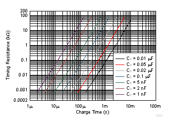
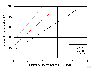
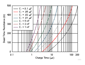
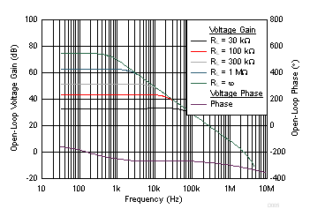
6.6 Typical Characteristics


