ZHCSOX6C September 2021 – December 2022 UCC14240-Q1
PRODUCTION DATA
- 1 特性
- 2 应用
- 3 说明
- 4 Revision History
- 5 Pin Configuration and Functions
-
6 Specifications
- 6.1 Absolute Maximum Ratings
- 6.2 ESD Ratings
- 6.3 Recommended Operating Conditions
- 6.4 Thermal Information
- 6.5 Power Ratings
- 6.6 Insulation Specifications
- 6.7 Safety-Related Certifications
- 6.8 Electrical Characteristics
- 6.9 Safety Limiting Values
- 6.10 Insulation Characteristics
- 6.11 Typical Characteristics
- 7 Detailed Description
- 8 Application and Implementation
- 9 Device and Documentation Support
- 10Mechanical, Packaging, and Orderable Information
8.2.3 Application Curves
The PMP23223 is a reference design that pairs the complementary UCC14240-Q1 isolated DC/DC power module with the UCC21732-Q1 isolated gate driver for a SiC power MOSFET or IGBT power module. The following waveforms show the controlled soft start for both positive and negative rails. Also shown, is the fast and highly accurate voltage regulation during gate driver switching from 1 kHz to 35 kHz. See PMP23223 reference design test report for more details.
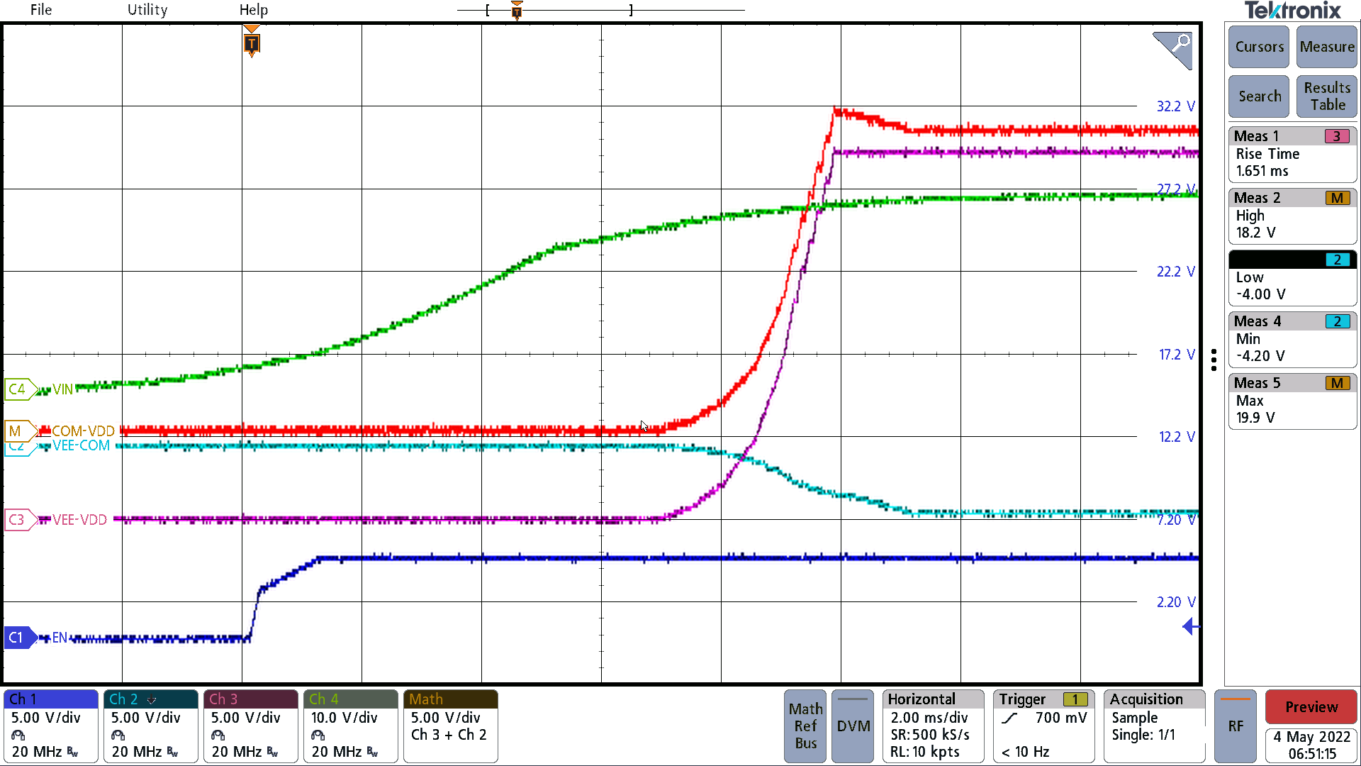 Figure 8-4 Power-Up Sequence.
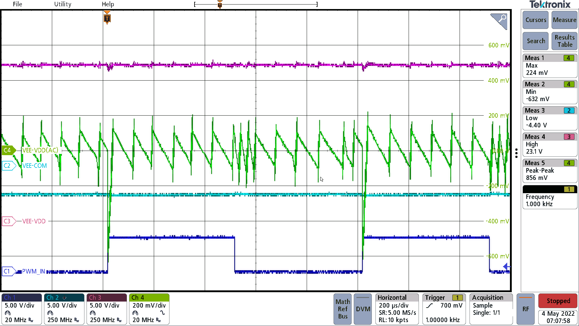 Figure 8-6 Ripple voltage: VDD-VEE Switching 100-nF Load at 1 kHz.
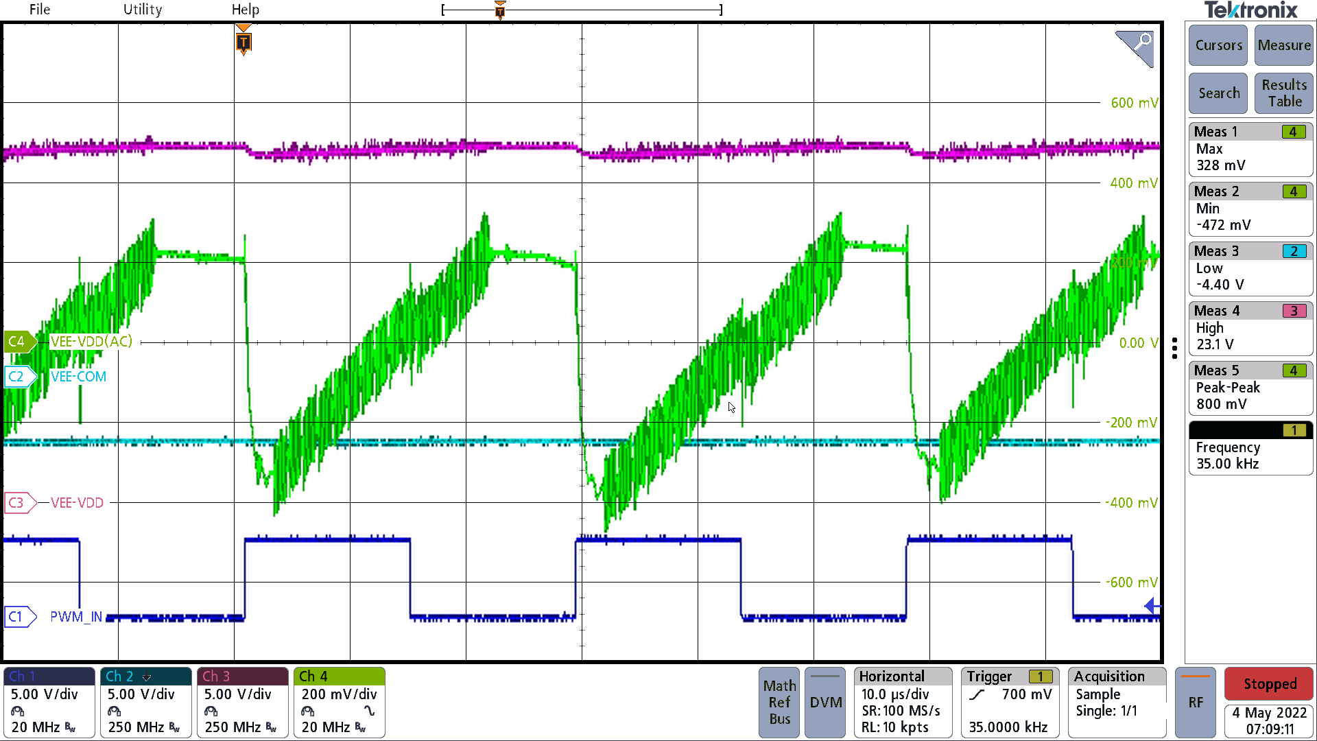 Figure 8-8 Ripple voltage: VDD-VEE Switching 100-nF Load at 35 kHz.
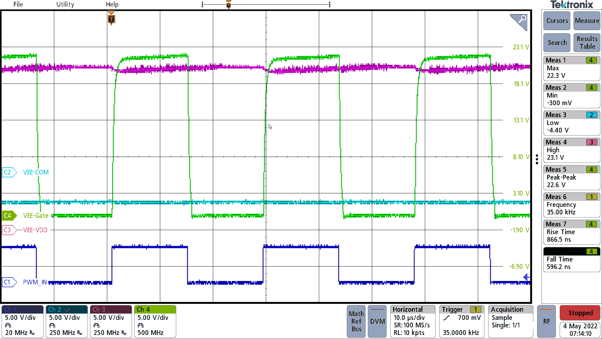 Figure 8-10 Gate Waveform Switching 100 nF at 35kHz.
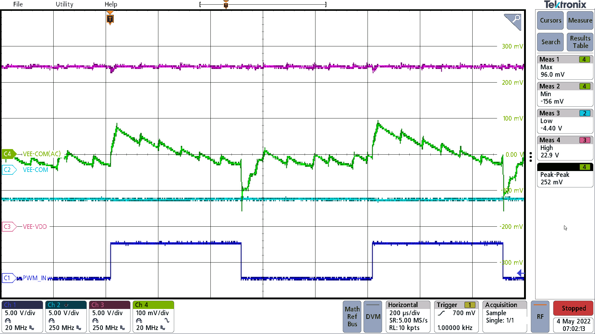 Figure 8-5 Ripple voltage: VEE-COM Switching 100-nF Load at 1 kHz.
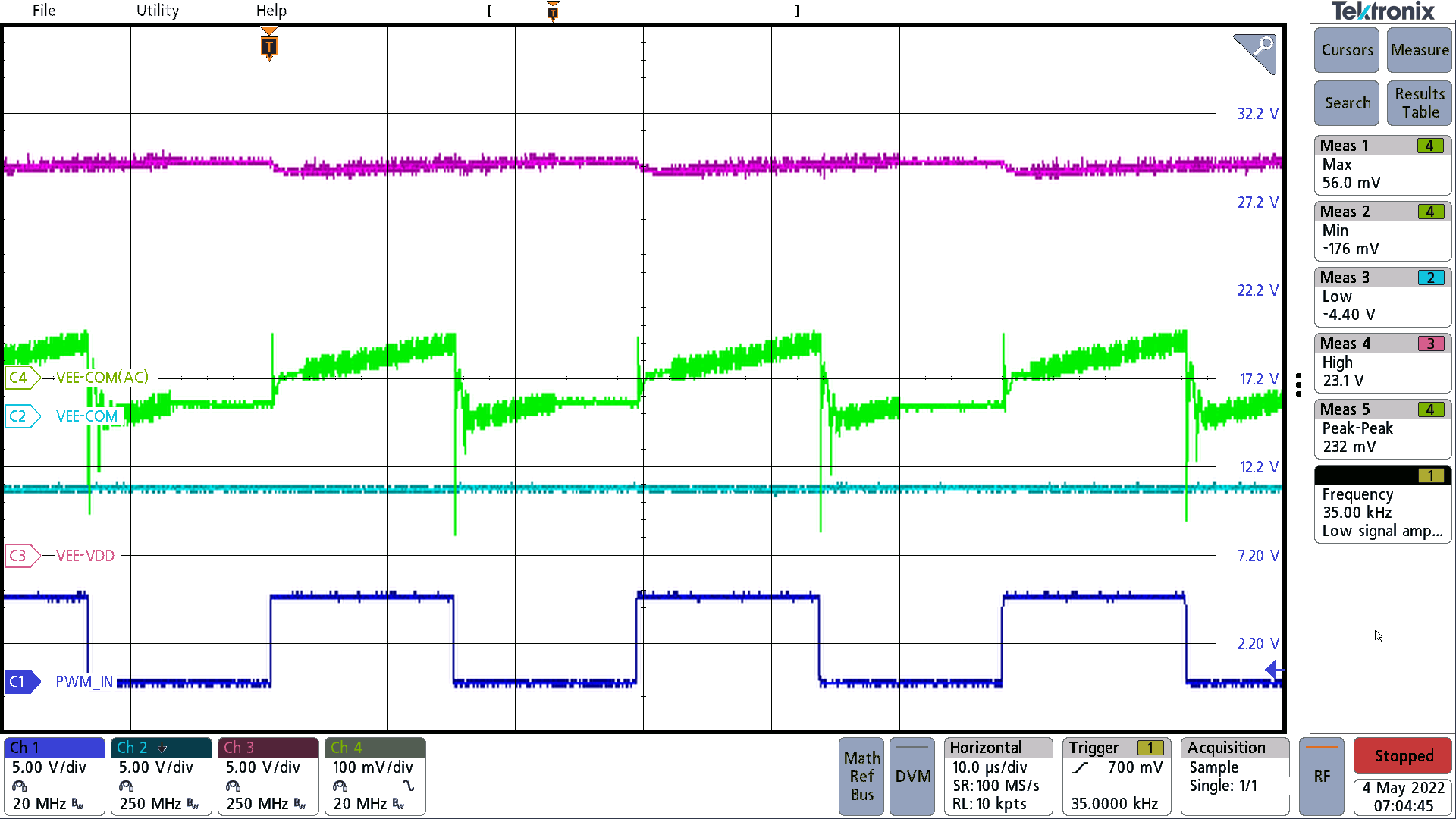 Figure 8-7 Ripple voltage: VEE-COM Switching 100-nF Load at 35 kHz.
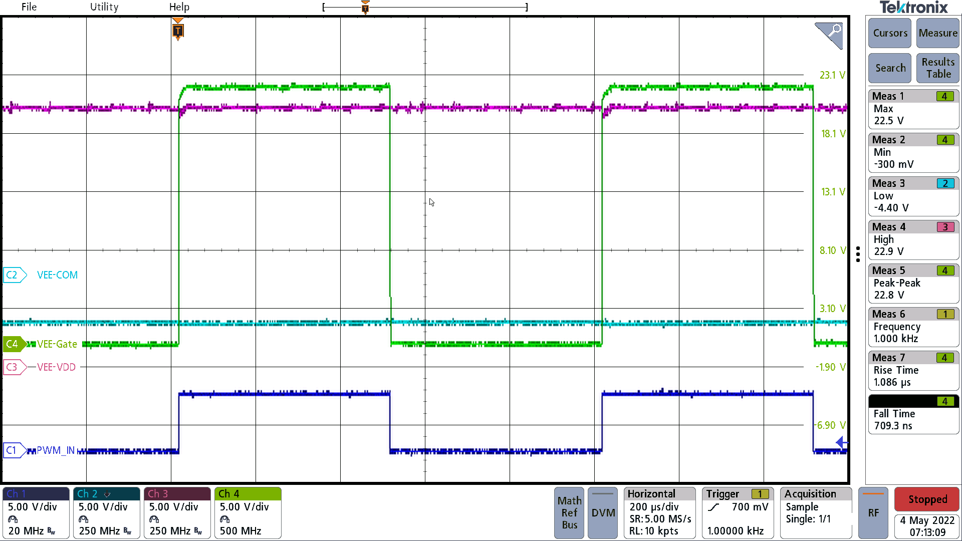 Figure 8-9 Gate Waveform Switching 100 nF at 1 kHz.