SLUS270G March 1999 – May 2020 UCC2800 , UCC2801 , UCC2802 , UCC2803 , UCC2804 , UCC2805
PRODUCTION DATA
- 1 Features
- 2 Applications
- 3 Description
- 4 Revision History
- 5 Description (continued)
- 6 Device Comparison Table
- 7 Pin Configuration and Functions
- 8 Specifications
-
9 Detailed Description
- 9.1 Overview
- 9.2 Functional Block Diagram
- 9.3
Feature Description
- 9.3.1 Detailed Pin Description
- 9.3.2 Undervoltage Lockout (UVLO)
- 9.3.3 Self-Biasing, Active Low Output
- 9.3.4 Reference Voltage
- 9.3.5 Oscillator
- 9.3.6 Synchronization
- 9.3.7 PWM Generator
- 9.3.8 Minimum Off-Time Setting (Dead-Time Control)
- 9.3.9 Leading Edge Blanking
- 9.3.10 Minimum Pulse Width
- 9.3.11 Current Limiting
- 9.3.12 Overcurrent Protection and Full Cycle Restart
- 9.3.13 Soft Start
- 9.3.14 Slope Compensation
- 9.4 Device Functional Modes
- 10Application and Implementation
- 11Power Supply Recommendations
- 12Layout
- 13Device and Documentation Support
- 14Mechanical, Packaging, and Orderable Information
9.3.10 Minimum Pulse Width
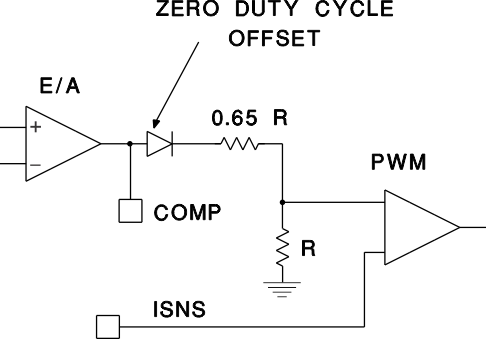
The leading edge blanking circuitry can lead to a minimum pulse width equal to the blanking interval under certain conditions. This occurs when the error amplifier output voltage (minus a diode drop and divided by 1.65) is lower than the current sense input. However, the amplifier output voltage must also be higher than a diode forward voltage drop of about 0.5 V. It is only during these conditions that a minimum output pulse width equal to the blanking duration can be obtained. Note that the PWM comparator has two inputs; one is from the current sense input. The other PWM input is the error amplifier output that has a diode and two resistors in series to ground. The diode in this network is used to ensure that zero duty cycle can be reached. Whenever the E/A output falls below a diode forward voltage drop, no current flows in the resistor divider and the PWM input goes to zero, along with pulse width.
 Figure 9-15 Zero Duty Cycle Offset