SLUS270G March 1999 – May 2020 UCC2800 , UCC2801 , UCC2802 , UCC2803 , UCC2804 , UCC2805
PRODUCTION DATA
- 1 Features
- 2 Applications
- 3 Description
- 4 Revision History
- 5 Description (continued)
- 6 Device Comparison Table
- 7 Pin Configuration and Functions
- 8 Specifications
-
9 Detailed Description
- 9.1 Overview
- 9.2 Functional Block Diagram
- 9.3
Feature Description
- 9.3.1 Detailed Pin Description
- 9.3.2 Undervoltage Lockout (UVLO)
- 9.3.3 Self-Biasing, Active Low Output
- 9.3.4 Reference Voltage
- 9.3.5 Oscillator
- 9.3.6 Synchronization
- 9.3.7 PWM Generator
- 9.3.8 Minimum Off-Time Setting (Dead-Time Control)
- 9.3.9 Leading Edge Blanking
- 9.3.10 Minimum Pulse Width
- 9.3.11 Current Limiting
- 9.3.12 Overcurrent Protection and Full Cycle Restart
- 9.3.13 Soft Start
- 9.3.14 Slope Compensation
- 9.4 Device Functional Modes
- 10Application and Implementation
- 11Power Supply Recommendations
- 12Layout
- 13Device and Documentation Support
- 14Mechanical, Packaging, and Orderable Information
9.3.5 Oscillator
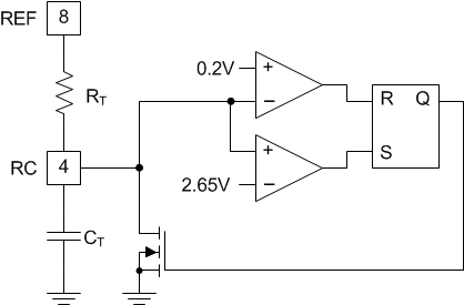
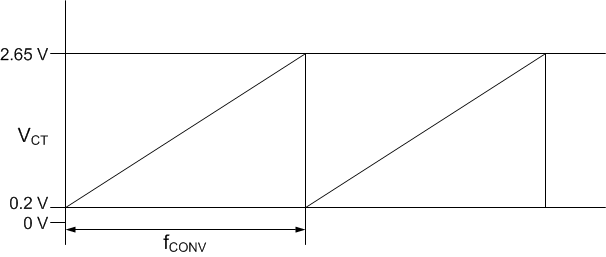
The UCC280x oscillator generates a sawtooth waveform on RC. The rise time is set by the time constant of RT and CT. The fall time is set by CT and an internal transistor on-resistance of approximately 130 Ω. During the fall time, the output is OFF and the maximum duty cycle is reduced below 50% or 100%, depending on the part number. Larger timing capacitors increase the discharge time and reduce the maximum duty cycle and frequency.
 Figure 9-6 Oscillator Equivalent Circuit
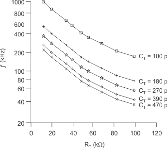
The oscillator section of the UCC2800 through UCC2805 BiCMOS devices has few similarities to the UC3842 type — other than single pin programming. It does still use a resistor to the reference voltage and capacitor to ground to program the oscillator frequency up to 1 MHz. Timing component values must be changed because a much lower charging current is desirable for low-power operation. Several characteristics of the oscillator have been optimized for high-speed, noise-immune operation. The oscillator peak-to-peak amplitude has been increased to 2.45 V typical versus 1.7 V on the UC3842 family. The lower oscillator threshold has been dropped to approximately 0.2 V while the upper threshold remains fairly close to the original 2.8 V at approximately
2.65 V.
Discharge current of the timing capacitor has been increased to nearly 20-mA peak as opposed to roughly 8 mA. This can be represented by approximately 130 Ω in series with the discharge switch to ground. A higher current was necessary to achieve brief dead times and high duty cycles with high-frequency operation. Practical applications can use these new ICs to a 1-MHz switching frequency.
 Figure 9-7 Oscillator Waveform
 Figure 9-8 Oscillator Frequency vs RT For Several CT