ZHCSGE2A
April 2017 – February 2018
UCC20225
PRODUCTION DATA.
1
特性
2
应用
3
说明
Device Images
功能方框图
4
修订历史记录
5
Pin Configuration and Functions
Pin Functions
6
Specifications
6.1
Absolute Maximum Ratings
6.2
ESD Ratings
6.3
Recommended Operating Conditions
6.4
Thermal Information
6.5
Power Ratings
6.6
Insulation Specifications
6.7
Safety-Related Certifications
6.8
Safety-Limiting Values
6.9
Electrical Characteristics
6.10
Switching Characteristics
6.11
Thermal Derating Curves
6.12
Typical Characteristics
7
Parameter Measurement Information
7.1
Propagation Delay and Pulse Width Distortion
7.2
Rising and Falling Time
7.3
PWM Input and Disable Response Time
7.4
Programable Dead Time
7.5
Power-up UVLO Delay to OUTPUT
7.6
CMTI Testing
8
Detailed Description
8.1
Overview
8.2
Functional Block Diagram
8.3
Feature Description
8.3.1
VDD, VCCI, and Under Voltage Lock Out (UVLO)
8.3.2
Input and Output Logic Table
8.3.3
Input Stage
8.3.4
Output Stage
8.3.5
Diode Structure in UCC20225
8.4
Device Functional Modes
8.4.1
Disable Pin
8.4.2
Programmable Dead Time (DT) Pin
8.4.2.1
Tying the DT Pin to VCC
8.4.2.2
DT Pin Left Open or Connected to a Programming Resistor between DT and GND Pins
9
Application and Implementation
9.1
Application Information
9.2
Typical Application
9.2.1
Design Requirements
9.2.2
Detailed Design Procedure
9.2.2.1
Designing PWM Input Filter
9.2.2.2
Select External Bootstrap Diode and its Series Resistor
9.2.2.3
Gate Driver Output Resistor
9.2.2.4
Estimate Gate Driver Power Loss
9.2.2.5
Estimating Junction Temperature
9.2.2.6
Selecting VCCI, VDDA/B Capacitor
9.2.2.6.1
Selecting a VCCI Capacitor
9.2.2.6.2
Selecting a VDDA (Bootstrap) Capacitor
9.2.2.6.3
Select a VDDB Capacitor
9.2.2.7
Dead Time Setting Guidelines
9.2.2.8
Application Circuits with Output Stage Negative Bias
9.2.3
Application Curves
10
Power Supply Recommendations
11
Layout
11.1
Layout Guidelines
11.2
Layout Example
12
器件和文档支持
12.1
文档支持
12.1.1
相关文档
12.2
认证
12.3
接收文档更新通知
12.4
社区资源
12.5
商标
12.6
静电放电警告
12.7
Glossary
13
机械、封装和可订购信息
封装选项
机械数据 (封装 | 引脚)
NPL|13
MPLG063A
散热焊盘机械数据 (封装 | 引脚)
订购信息
zhcsge2a_oa
6.12
Typical Characteristics
VDDA = VDDB= 12 V, VCCI = 3.3 V, T
A
= 25°C, No load unless otherwise noted.
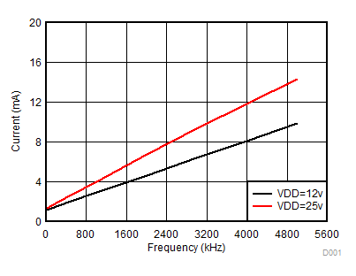
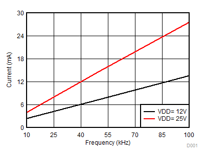
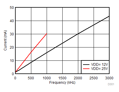
Figure 4.
Per Channel Current Consumption vs. Frequency (No Load, VDD = 12 V or 25 V)
Figure 6.
Per Channel Current Consumption (I
VDDA/B
) vs. Frequency (10-nF Load, VDD = 12 V or 25 V)
Figure 8.
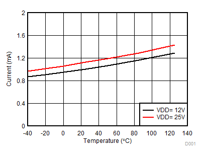
Per Channel (I
VDDA/B
) Quiescent Supply Current vs Temperature (No Load, Input Low, No Switching)
A.
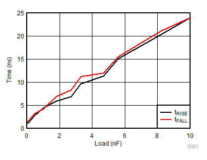
Figure 10.
Rising and Falling Times vs. Load (VDD = 12 V)
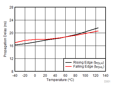
Figure 12.
Propagation Delay vs. Temperature
A.
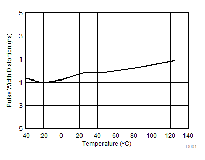
Figure 14.
Pulse Width Distortion vs. Temperature
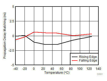
Figure 16.
Propagation Delay Matching (t
DM
) vs. Temperature
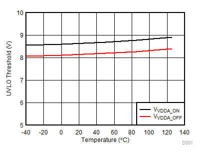
Figure 18.
VDD UVLO Threshold vs. Temperature
Figure 20.
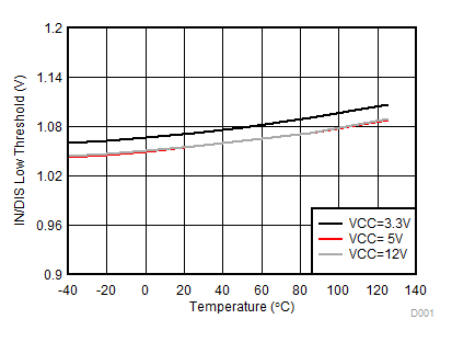
PWM/DIS Low Threshold
Figure 22.
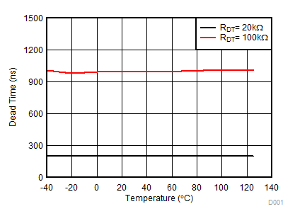
Dead Time vs. Temperature (with R
DT
= 20 kΩ and 100 kΩ)
Figure 5.
Per Channel Current Consumption (I
VDDA/B
) vs. Frequency (1-nF Load, VDD = 12 V or 25 V)
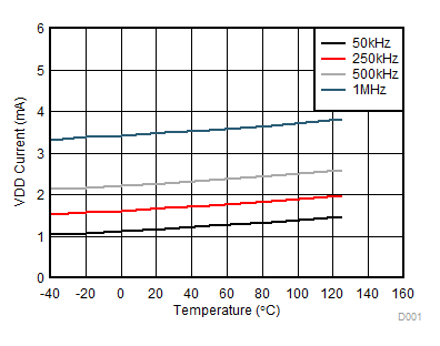
Figure 7.
Per Channel (I
VDDA/B
) Supply Current Vs. Temperature (No Load, Different Switching Frequencies)
A.
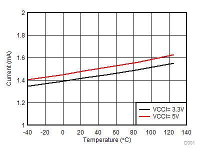
Figure 9.
I
VCCI
Quiescent Supply Current vs Temperature (No Load, DIS is High, No Switching)
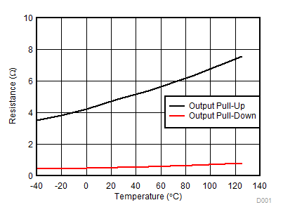
Figure 11.
Output Resistance vs. Temperature
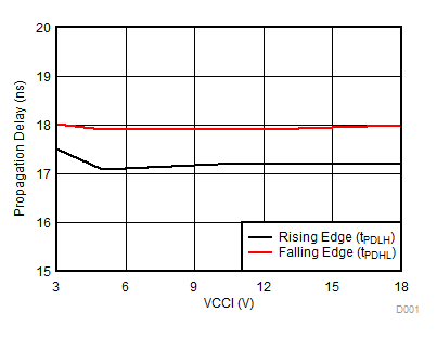
Figure 13.
Propagation Delay vs. VCCI
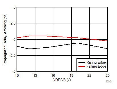
Figure 15.
Propagation Delay Matching (t
DM
) vs. VDD
Figure 17.
VDD UVLO Hysteresis vs. Temperature
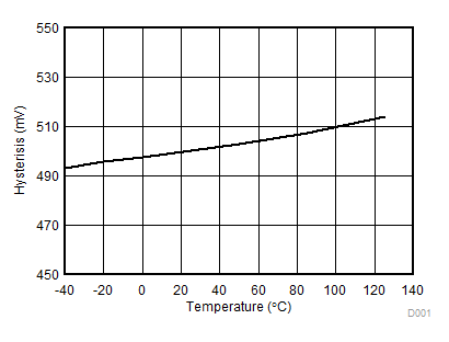
Figure 19.
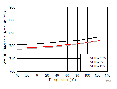
PWM/DIS Hysteresis vs. Temperature
Figure 21.
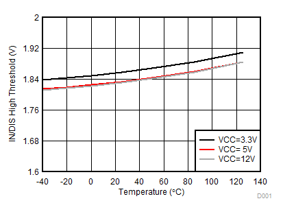
PWM/DIS High Threshold
Figure 23.
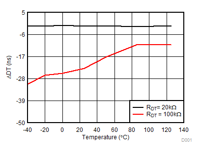
Dead Time Matching vs. Temperature (with R
DT
= 20 kΩ and 100 kΩ)
千亿体育app官网登录(中国)官方网站IOS/安卓通用版/手机APP
|
米乐app下载官网(中国)|ios|Android/通用版APP最新版
|
米乐|米乐·M6(中国大陆)官方网站
|
千亿体育登陆地址
|
华体会体育(中国)HTH·官方网站
|
千赢qy国际_全站最新版千赢qy国际V6.2.14安卓/IOS下载
|
18新利网v1.2.5|中国官方网站
|
bob电竞真人(中国官网)安卓/ios苹果/电脑版【1.97.95版下载】
|
千亿体育app官方下载(中国)官方网站IOS/安卓/手机APP下载安装
|