ZHCSFN1A November 2016 – January 2022 UCC20520
PRODUCTION DATA
- 1 特性
- 2 应用
- 3 说明
- 4 Revision History
- 5 Pin Configuration and Functions
-
6 Specifications
- 6.1 Absolute Maximum Ratings
- 6.2 ESD Ratings
- 6.3 Recommended Operating Conditions
- 6.4 Thermal Information
- 6.5 Power Ratings
- 6.6 Insulation Specifications
- 6.7 Safety-Related Certifications
- 6.8 Safety-Limiting Values
- 6.9 Electrical Characteristics
- 6.10 Switching Characteristics
- 6.11 Insulation Characteristics Curves
- 6.12 Typical Characteristics
- 7 Parameter Measurement Information
- 8 Detailed Description
-
9 Application and Implementation
- 9.1 Application Information
- 9.2
Typical Application
- 9.2.1 Design Requirements
- 9.2.2
Detailed Design Procedure
- 9.2.2.1 Designing PWM Input Filter
- 9.2.2.2 Select External Bootstrap Diode and its Series Resistor
- 9.2.2.3 Gate Driver Output Resistor
- 9.2.2.4 Estimate Gate Driver Power Loss
- 9.2.2.5 Estimating Junction Temperature
- 9.2.2.6 Selecting VCCI, VDDA/B Capacitor
- 9.2.2.7 Dead Time Setting Guidelines
- 9.2.2.8 Application Circuits with Output Stage Negative Bias
- 9.2.2.9 56
- 9.2.3 Application Curves
- 10Layout
- 11Device and Documentation Support
5 Pin Configuration and Functions
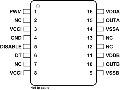
 Figure 5-1 DW Package, 16-Pin SOIC (Top View)
Table 5-1 Pin Functions
| PIN | TYPE1 | DESCRIPTION | |
|---|---|---|---|
| NAME | NO. | ||
| DISABLE | 5 | I | Disables both driver outputs if asserted high, enables if set low or left open. This pin is pulled low internally if left open. It is recommended to tie this pin to ground if not used to achieve better noise immunity. |
| DT | 6 | I | Programmable dead time function. Tying DT to VCCI disables the DT function with dead time ≅ 0 ns. Leaving DT open sets the dead time to <15 ns. Placing a 500-Ω to 500-kΩ resistor (RDT) between DT and GND adjusts dead time according to: DT (in ns) = 10 × RDT (in kΩ). It is recommended to parallel a ceramic capacitor, ≥2.2-nF, with RDT to achieve better noise immunity. |
| GND | 4 | P | Primary-side ground reference. All signals in the primary side are referenced to this ground. |
| NC | 2 | – | No connection. |
| NC | 7 | – | No connection. |
| NC | 12 | – | No connection. |
| NC | 13 | – | No connection. |
| OUTA | 15 | O | Output of driver A. Connect to the gate of the A channel FET or IGBT. Output A is in phase with PWM input with a propagation delay |
| OUTB | 10 | O | Output of driver B. Connect to the gate of the B channel FET or IGBT. Output B is always complementary to output A with a programmed dead time. |
| PWM | 1 | I | PWM input has a TTL/CMOS compatible input threshold. This pin is pulled low internally if left open. |
| VCCI | 3 | P | Primary-side supply voltage. Locally decoupled to GND using a low ESR/ESL capacitor located as close to the device as possible. |
| VCCI | 8 | P | Primary-side supply voltage. This pin is internally shorted to pin 3. |
| VDDA | 16 | P | Secondary-side power for driver A. Locally decoupled to VSSA using a low ESR/ESL capacitor located as close to the device as possible. |
| VDDB | 11 | P | Secondary-side power for driver B. Locally decoupled to VSSB using a low ESR/ESL capacitor located as close to the device as possible. |
| VSSA | 14 | P | Ground for secondary-side driver A. Ground reference for secondary side A channel. |
| VSSB | 9 | P | Ground for secondary-side driver B. Ground reference for secondary side B channel. |
- I = input, O = output, I/O = input or output, FB = feedback, G = ground, P = power