SLUSCV6A April 2017 – February 2018 UCC21225A
PRODUCTION DATA.
- 1 Features
- 2 Applications
- 3 Description
- 4 Revision History
- 5 Pin Configuration and Functions
-
6 Specifications
- 6.1 Absolute Maximum Ratings
- 6.2 ESD Ratings
- 6.3 Recommended Operating Conditions
- 6.4 Thermal Information
- 6.5 Power Ratings
- 6.6 Insulation Specifications
- 6.7 Safety-Related Certifications
- 6.8 Safety-Limiting Values
- 6.9 Electrical Characteristics
- 6.10 Switching Characteristics
- 6.11 Insulation Characteristics and Thermal Derating Curves
- 6.12 Typical Characteristics
- 7 Parameter Measurement Information
- 8 Detailed Description
-
9 Application and Implementation
- 9.1 Application Information
- 9.2
Typical Application
- 9.2.1 Design Requirements
- 9.2.2
Detailed Design Procedure
- 9.2.2.1 Designing INA/INB Input Filter
- 9.2.2.2 Select External Bootstrap Diode and Series Resistor
- 9.2.2.3 Gate Driver Output Resistor
- 9.2.2.4 Estimate Gate Driver Power Loss
- 9.2.2.5 Estimating Junction Temperature
- 9.2.2.6 Selecting VCCI, VDDA/B Capacitor
- 9.2.2.7 Dead Time Setting Guidelines
- 9.2.2.8 Application Circuits with Output Stage Negative Bias
- 9.2.3 Application Curves
- 10Power Supply Recommendations
- 11Layout
- 12Device and Documentation Support
- 13Mechanical, Packaging, and Orderable Information
6.12 Typical Characteristics
VDDA = VDDB = 12 V, VCCI = 3.3 V, TA = 25°C, No load unless otherwise noted.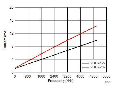
Figure 4. Per Channel Current Consumption vs. Frequency (No Load, VDD = 12 V or 25 V)
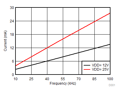
Figure 6. Per Channel Current Consumption (IVDDA/B) vs. Frequency (10-nF Load, VDD = 12 V or 25 V)
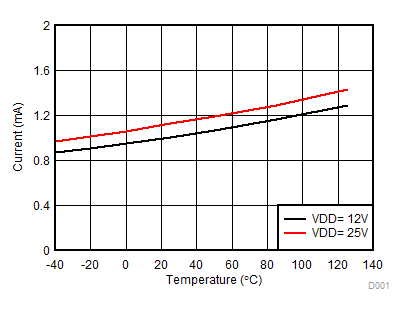
Figure 8. Per Channel (IVDDA/B) Quiescent Supply Current vs Temperature (No Load, Input Low, No Switching)
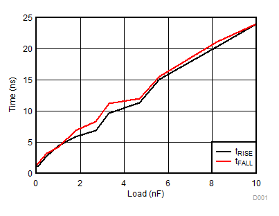
A.
Figure 10. Rising and Falling Times vs. Load (VDD = 12 V)
Figure 12. Propagation Delay vs. Temperature
A.
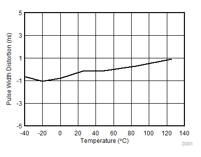
Figure 14. Pulse Width Distortion vs. Temperature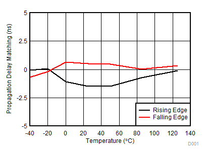
Figure 16. Propagation Delay Matching (tDM) vs. Temperature
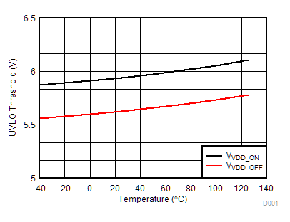
Figure 18. VDD UVLO Threshold vs. Temperature

Figure 20. IN/DIS Low Threshold
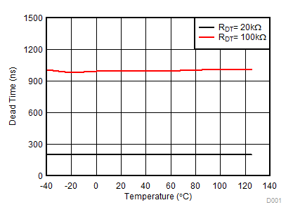
Figure 22. Dead Time vs. Temperature (with RDT = 20 kΩ and 100 kΩ)

Figure 5. Per Channel Current Consumption (IVDDA/B) vs. Frequency (1-nF Load, VDD = 12 V or 25 V)
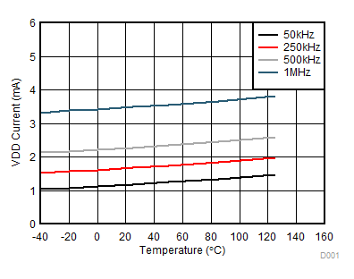
Figure 7. Per Channel (IVDDA/B) Supply Current Vs. Temperature (No Load, Different Switching Frequencies)
A.
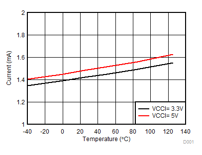
Figure 9. IVCCI Quiescent Supply Current vs Temperature (No Load, Input Low, No Switching)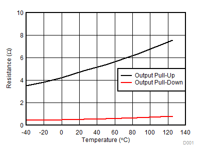
Figure 11. Output Resistance vs. Temperature
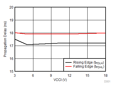
Figure 13. Propagation Delay vs. VCCI
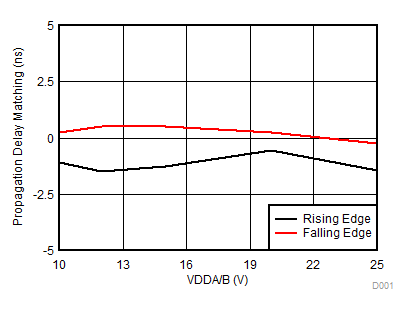
Figure 15. Propagation Delay Matching (tDM) vs. VDD
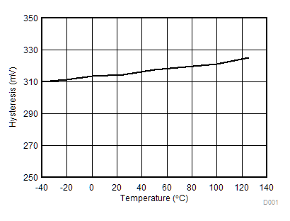
Figure 17. VDD UVLO Hysteresis vs. Temperature
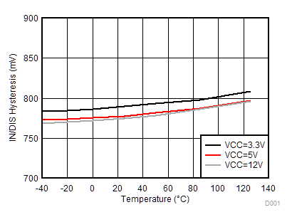
Figure 19. IN/DIS Hysteresis vs. Temperature
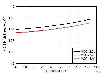
Figure 21. IN/DIS High Threshold
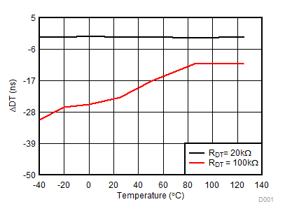
Figure 23. Dead Time Matching vs. Temperature (with RDT = 20 kΩ and 100 kΩ)