SLUSCV6A April 2017 – February 2018 UCC21225A
PRODUCTION DATA.
- 1 Features
- 2 Applications
- 3 Description
- 4 Revision History
- 5 Pin Configuration and Functions
-
6 Specifications
- 6.1 Absolute Maximum Ratings
- 6.2 ESD Ratings
- 6.3 Recommended Operating Conditions
- 6.4 Thermal Information
- 6.5 Power Ratings
- 6.6 Insulation Specifications
- 6.7 Safety-Related Certifications
- 6.8 Safety-Limiting Values
- 6.9 Electrical Characteristics
- 6.10 Switching Characteristics
- 6.11 Insulation Characteristics and Thermal Derating Curves
- 6.12 Typical Characteristics
- 7 Parameter Measurement Information
- 8 Detailed Description
-
9 Application and Implementation
- 9.1 Application Information
- 9.2
Typical Application
- 9.2.1 Design Requirements
- 9.2.2
Detailed Design Procedure
- 9.2.2.1 Designing INA/INB Input Filter
- 9.2.2.2 Select External Bootstrap Diode and Series Resistor
- 9.2.2.3 Gate Driver Output Resistor
- 9.2.2.4 Estimate Gate Driver Power Loss
- 9.2.2.5 Estimating Junction Temperature
- 9.2.2.6 Selecting VCCI, VDDA/B Capacitor
- 9.2.2.7 Dead Time Setting Guidelines
- 9.2.2.8 Application Circuits with Output Stage Negative Bias
- 9.2.3 Application Curves
- 10Power Supply Recommendations
- 11Layout
- 12Device and Documentation Support
- 13Mechanical, Packaging, and Orderable Information
8.3.1 VDD, VCCI, and Under Voltage Lock Out (UVLO)
The UCC21225A has an internal under voltage lock out (UVLO) protection feature on the supply circuit blocks between the VDD and VSS pins for both outputs. When the VDD bias voltage is lower than VVDD_ON at device start-up or lower than VVDD_OFF after start-up, the VDD UVLO feature holds the effected output low, regardless of the status of the input pins (INA and INB).
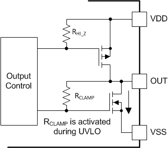
When the output stages of the driver are in an unbiased or UVLO condition, the driver outputs are held low by an active clamp circuit that limits the voltage rise on the driver outputs (Illustrated in Figure 31 ). In this condition, the upper PMOS is resistively held off by RHi-Z while the lower NMOS gate is tied to the driver output through RCLAMP. In this configuration, the output is effectively clamped to the threshold voltage of the lower NMOS device, typically around 1.5-V, when no bias power is available. The clamp sinking current is limited only by the per-channel safety supply power, the ambient temperature, and the 6-A peak sink current rating.
 Figure 31. Simplified Representation of Active Pull Down Feature
The VDD UVLO protection has a hysteresis feature (VVDD_HYS). This hysteresis prevents chatter when there is ground noise from the power supply. This also allows the device to accept small drops in bias voltage, which occurs when the device starts switching and operating current consumption increases suddenly.
The input side of the UCC21225A also has an internal under voltage lock out (UVLO) protection feature. The device isn't active unless the voltage at VCCI exceeds VVCCI_ON. A signal will cease to be delivered when VCCI receives a voltage less than VVCCI_OFF. As with the UVLO for VDD, there is hystersis (VVCCI_HYS) to ensure stable operation.
If INA or INB are active before VCCI or VDD have crossed above their respective on thresholds, the output will not update until 50-µs (typical) after VCCI or VDD crossing its UVLO rising threshold. However, when either VCCI or VDD receive a voltage less than their respective off thresholds, there is <1-µs delay, depending on the voltage slew rate on the supply pins, before the outputs are held low. This asymmetric delay is designed to ensure safe operation during VCCI or VDD brownouts.
The UCC21225A can withstand an absolute maximum of 30 V for VDD, and 20 V for VCCI.
Table 1. UCC21225A VCCI UVLO Feature Logic
| CONDITION | INPUTS | OUTPUTS | ||
| INA | INB | OUTA | OUTB | |
| VCCI-GND < VVCCI_ON during device start up | H | L | L | L |
| VCCI-GND < VVCCI_ON during device start up | L | H | L | L |
| VCCI-GND < VVCCI_ON during device start up | H | H | L | L |
| VCCI-GND < VVCCI_ON during device start up | L | L | L | L |
| VCCI-GND < VVCCI_OFF after device start up | H | L | L | L |
| VCCI-GND < VVCCI_OFF after device start up | L | H | L | L |
| VCCI-GND < VVCCI_OFF after device start up | H | H | L | L |
| VCCI-GND < VVCCI_OFF after device start up | L | L | L | L |
Table 2. UCC21225A VDD UVLO Feature Logic
| CONDITION | INPUTS | OUTPUTS | ||
| INA | INB | OUTA | OUTB | |
| VDD-VSS < VVDD_ON during device start up | H | L | L | L |
| VDD-VSS < VVDD_ON during device start up | L | H | L | L |
| VDD-VSS < VVDD_ON during device start up | H | H | L | L |
| VDD-VSS < VVDD_ON during device start up | L | L | L | L |
| VDD-VSS < VVDD_OFF after device start up | H | L | L | L |
| VDD-VSS < VVDD_OFF after device start up | L | H | L | L |
| VDD-VSS < VVDD_OFF after device start up | H | H | L | L |
| VDD-VSS < VVDD_OFF after device start up | L | L | L | L |