ZHCSGY8B October 2017 – July 2018 UCC21520-Q1
UNLESS OTHERWISE NOTED, this document contains PRODUCTION DATA.
- 1 特性
- 2 应用
- 3 说明
- 4 修订历史记录
- 5 Pin Configuration and Functions
-
6 Specifications
- 6.1 Absolute Maximum Ratings
- 6.2 ESD Ratings
- 6.3 Recommended Operating Conditions
- 6.4 Thermal Information
- 6.5 Power Ratings
- 6.6 Insulation Specifications
- 6.7 Safety-Related Certifications
- 6.8 Safety-Limiting Values
- 6.9 Electrical Characteristics
- 6.10 Switching Characteristics
- 6.11 Insulation Characteristics Curves
- 6.12 Typical Characteristics
- 7 Parameter Measurement Information
- 8 Detailed Description
-
9 Application and Implementation
- 9.1 Application Information
- 9.2
Typical Application
- 9.2.1 Design Requirements
- 9.2.2
Detailed Design Procedure
- 9.2.2.1 Designing INA/INB Input Filter
- 9.2.2.2 Select External Bootstrap Diode and its Series Resistor
- 9.2.2.3 Gate Driver Output Resistor
- 9.2.2.4 Estimate Gate Driver Power Loss
- 9.2.2.5 Estimating Junction Temperature
- 9.2.2.6 Selecting VCCI, VDDA/B Capacitor
- 9.2.2.7 Dead Time Setting Guidelines
- 9.2.2.8 Application Circuits with Output Stage Negative Bias
- 9.2.3 Application Curves
- 10Power Supply Recommendations
- 11Layout
- 12器件和文档支持
- 13机械、封装和可订购信息
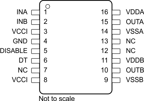
5 Pin Configuration and Functions
DW Package
16-Pin SOIC
Top View

Pin Functions
| PIN | I/O(1) | DESCRIPTION | |
|---|---|---|---|
| NAME | NO. | ||
| DISABLE | 5 | I | Disables both driver outputs if asserted high, enables if set low or left open. This pin is pulled low internally if left open. It is recommended to tie this pin to ground if not used to achieve better noise immunity. Bypass using a ≈1nF low ESR/ESL capacitor close to DIS pin when connecting to a micro controller with distance. |
| DT | 6 | I | Programmable dead time function.
Tying DT to VCCI allows the outputs to overlap. Leaving DT open sets the dead time to <15 ns. Placing a 500-Ω to 500-kΩ resistor (RDT) between DT and GND adjusts dead time according to: DT (in ns) = 10 x RDT (in kΩ). It is recommended to parallel a ceramic capacitor, 2.2 nF or above, close to the DT pin with RDT to achieve better noise immunity. |
| GND | 4 | P | Primary-side ground reference. All signals in the primary side are referenced to this ground. |
| INA | 1 | I | Input signal for A channel. INA input has a TTL/CMOS compatible input threshold. This pin is pulled low internally if left open. It is recommended to tie this pin to ground if not used to achieve better noise immunity. |
| INB | 2 | I | Input signal for B channel. INB input has a TTL/CMOS compatible input threshold. This pin is pulled low internally if left open. It is recommended to tie this pin to ground if not used to achieve better noise immunity. |
| NC | 7 | – | No Internal connection. |
| NC | 12 | – | No internal connection. |
| NC | 13 | – | No internal connection. |
| OUTA | 15 | O | Output of driver A. Connect to the gate of the A channel FET or IGBT. |
| OUTB | 10 | O | Output of driver B. Connect to the gate of the B channel FET or IGBT. |
| VCCI | 3 | P | Primary-side supply voltage. Locally decoupled to GND using a low ESR/ESL capacitor located as close to the device as possible. |
| VCCI | 8 | P | Primary-side supply voltage. This pin is internally shorted to pin 3. |
| VDDA | 16 | P | Secondary-side power for driver A. Locally decoupled to VSSA using a low ESR/ESL capacitor located as close to the device as possible. |
| VDDB | 11 | P | Secondary-side power for driver B. Locally decoupled to VSSB using low ESR/ESL capacitor located as close to the device as possible. |
| VSSA | 14 | P | Ground for secondary-side driver A. Ground reference for secondary side A channel. |
| VSSB | 9 | P | Ground for secondary-side driver B. Ground reference for secondary side B channel. |
(1) P =Power, G= Ground, I= Input, O= Output