ZHCSGY8B October 2017 – July 2018 UCC21520-Q1
UNLESS OTHERWISE NOTED, this document contains PRODUCTION DATA.
- 1 特性
- 2 应用
- 3 说明
- 4 修订历史记录
- 5 Pin Configuration and Functions
-
6 Specifications
- 6.1 Absolute Maximum Ratings
- 6.2 ESD Ratings
- 6.3 Recommended Operating Conditions
- 6.4 Thermal Information
- 6.5 Power Ratings
- 6.6 Insulation Specifications
- 6.7 Safety-Related Certifications
- 6.8 Safety-Limiting Values
- 6.9 Electrical Characteristics
- 6.10 Switching Characteristics
- 6.11 Insulation Characteristics Curves
- 6.12 Typical Characteristics
- 7 Parameter Measurement Information
- 8 Detailed Description
-
9 Application and Implementation
- 9.1 Application Information
- 9.2
Typical Application
- 9.2.1 Design Requirements
- 9.2.2
Detailed Design Procedure
- 9.2.2.1 Designing INA/INB Input Filter
- 9.2.2.2 Select External Bootstrap Diode and its Series Resistor
- 9.2.2.3 Gate Driver Output Resistor
- 9.2.2.4 Estimate Gate Driver Power Loss
- 9.2.2.5 Estimating Junction Temperature
- 9.2.2.6 Selecting VCCI, VDDA/B Capacitor
- 9.2.2.7 Dead Time Setting Guidelines
- 9.2.2.8 Application Circuits with Output Stage Negative Bias
- 9.2.3 Application Curves
- 10Power Supply Recommendations
- 11Layout
- 12器件和文档支持
- 13机械、封装和可订购信息
9.2.3 Application Curves
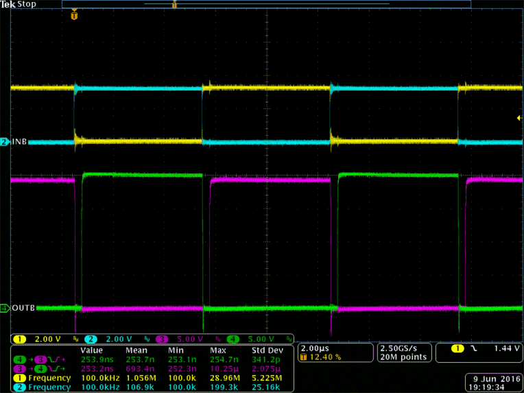
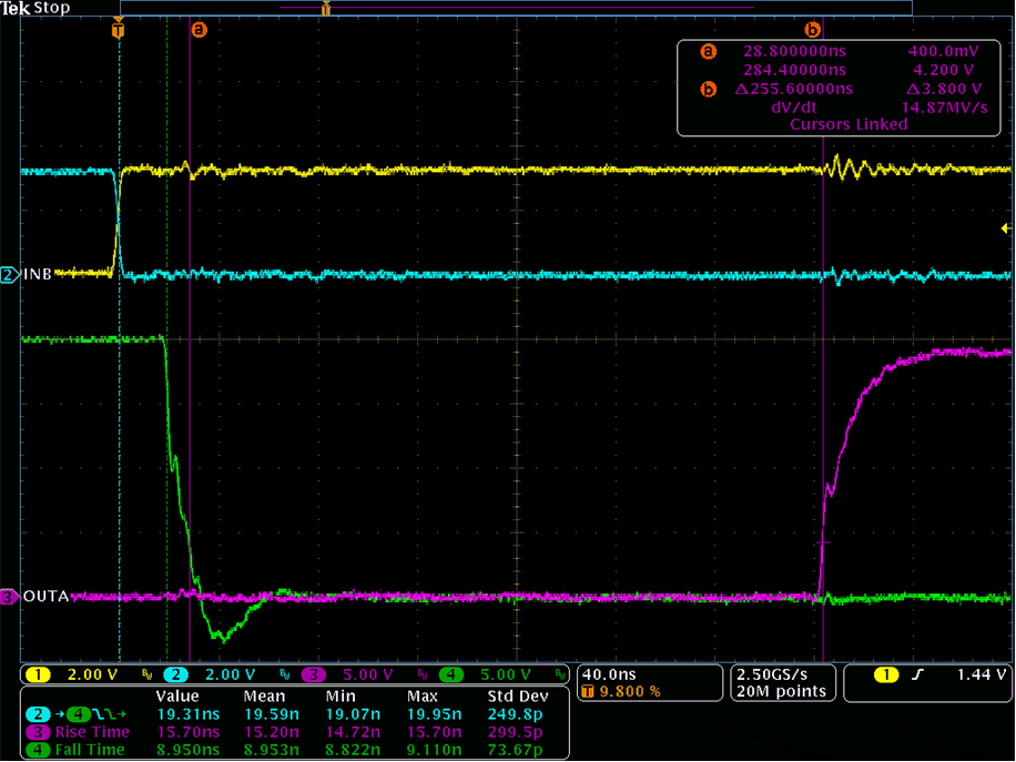
Figure 42 and Figure 43 shows the bench test waveforms for the design example shown in Figure 38 under these conditions: VCC = 5 V, VDD = 20 V, fSW = 100 kHz, VDC-Link = 0 V.
Channel 1 (Yellow): UCC21520-Q1 INA pin signal.
Channel 2 (Blue): UCC21520-Q1 INB pin signal.
Channel 3 (Pink): Gate-source signal on the high side power transistor.
Channel 4 (Green): Gate-source signal on the low side power transistor.
In Figure 42, INA and INB are sent complimentary 3.3-V, 50% duty-cycle signals. The gate drive signals on the power transistor have a 250-ns dead time, shown in the measurement section of Figure 42. The dead-time matching is less than 1 ns with the 250-ns dead-time setting.
Figure 43 shows a zoomed-in version of the waveform of Figure 42, with measurements for propagation delay and rising/falling time. Cursors are also used to measure dead time. Importantly, the output waveform is measured between the power transistors’ gate and source pins, and is not measured directly from the driver OUTA and OUTB pins. Due to the split on and off resistors (Ron,Roff) and different sink and source currents, different rising (16 ns) and falling time (9 ns) are observed in Figure 43.

