SLUSDE1E September   2018  – November 2024 UCC21540 , UCC21540A , UCC21541 , UCC21542

PRODUCTION DATA  

  1.   1
  2. Features
  3. Applications
  4. Description
  5. Device Comparison Table
  6. Pin Configuration and Functions
    1. 5.1 Pin Configuration and Functions
    2. 5.2 UCC21542 Pin Functions
  7. Specifications
    1. 6.1  Absolute Maximum Ratings
    2. 6.2  ESD Ratings
    3. 6.3  Recommended Operating Conditions
    4. 6.4  Thermal Information
    5. 6.5  Power Ratings
    6. 6.6  Insulation Specifications
    7. 6.7  Safety-Limiting Values
    8. 6.8  Electrical Characteristics
    9. 6.9  Switching Characteristics
    10. 6.10 Insulation Characteristics Curves
    11. 6.11 Typical Characteristics
  8. Parameter Measurement Information
    1. 7.1 Minimum Pulses
    2. 7.2 Propagation Delay and Pulse Width Distortion
    3. 7.3 Rising and Falling Time
    4. 7.4 Input and Disable Response Time
    5. 7.5 Programmable Dead Time
    6. 7.6 Power-Up UVLO Delay to OUTPUT
    7. 7.7 CMTI Testing
  9. Detailed Description
    1. 8.1 Overview
    2. 8.2 Functional Block Diagram
    3. 8.3 Feature Description
      1. 8.3.1 VDD, VCCI, and Under Voltage Lock Out (UVLO)
      2. 8.3.2 Input and Output Logic Table
      3. 8.3.3 Input Stage
      4. 8.3.4 Output Stage
      5. 8.3.5 Diode Structure in the UCC2154x
    4. 8.4 Device Functional Modes
      1. 8.4.1 Disable Pin
      2. 8.4.2 Programmable Dead Time (DT) Pin
        1. 8.4.2.1 DT Pin Tied to VCCI
        2. 8.4.2.2 Connecting a Programming Resistor between DT and GND Pins
  10. Application and Implementation
    1. 9.1 Application Information
    2. 9.2 Typical Application
      1. 9.2.1 Design Requirements
      2. 9.2.2 Detailed Design Procedure
        1. 9.2.2.1 Designing INA/INB Input Filter
        2. 9.2.2.2 Select Dead Time Resistor and Capacitor
        3. 9.2.2.3 Select External Bootstrap Diode and Its Series Resistor
        4. 9.2.2.4 Gate Driver Output Resistor
        5. 9.2.2.5 Gate to Source Resistor Selection
        6. 9.2.2.6 Estimating Gate Driver Power Loss
        7. 9.2.2.7 Estimating Junction Temperature
        8. 9.2.2.8 Selecting VCCI, VDDA/B Capacitor
          1. 9.2.2.8.1 Selecting a VCCI Capacitor
          2. 9.2.2.8.2 Selecting a VDDA (Bootstrap) Capacitor
          3. 9.2.2.8.3 Select a VDDB Capacitor
        9. 9.2.2.9 Application Circuits with Output Stage Negative Bias
      3. 9.2.3 Application Curves
  11. 10Power Supply Recommendations
  12. 11Layout
    1. 11.1 Layout Guidelines
      1. 11.1.1 Component Placement Considerations
      2. 11.1.2 Grounding Considerations
      3. 11.1.3 High-Voltage Considerations
      4. 11.1.4 Thermal Considerations
    2. 11.2 Layout Example
  13. 12Device and Documentation Support
    1. 12.1 Third-Party Products Disclaimer
    2. 12.2 Documentation Support
      1. 12.2.1 Related Documentation
    3. 12.3 Receiving Notification of Documentation Updates
    4. 12.4 Support Resources
    5. 12.5 Trademarks
    6. 12.6 Electrostatic Discharge Caution
    7. 12.7 Glossary
  14. 13Revision History
  15. 14Mechanical, Packaging, and Orderable Information

封装选项

请参考 PDF 数据表获取器件具体的封装图。

机械数据 (封装 | 引脚)
  • DW|16
散热焊盘机械数据 (封装 | 引脚)
订购信息

Insulation Characteristics Curves

UCC21540 UCC21540A UCC21541 UCC21542 Reinforced Isolation Capacitor Life Time ProjectionFigure 6-1 Reinforced Isolation Capacitor Life Time Projection
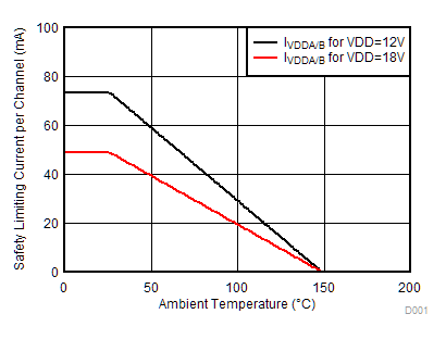
UCC21540 UCC21540A UCC21541 UCC21542 Thermal Derating Curve for Limiting Current Per
                        VDE,
                        DWK Package
Current in Each Channel with Both Channels Running Simultaneously
Figure 6-2 Thermal Derating Curve for Limiting Current Per VDE, DWK Package
UCC21540 UCC21540A UCC21541 UCC21542 Thermal Derating Curve
                        for Limiting Current Per
                        VDE,
                        DW Package
Current in Each Channel with Both Channels Running Simultaneously
Figure 6-4 Thermal Derating Curve for Limiting Current Per VDE, DW Package
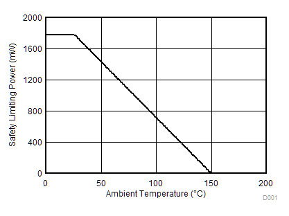
UCC21540 UCC21540A UCC21541 UCC21542 Thermal Derating Curve for Limiting Power Per
                        VDE,
                        DWK Package
Figure 6-3 Thermal Derating Curve for Limiting Power Per VDE, DWK Package
UCC21540 UCC21540A UCC21541 UCC21542 Thermal Derating Curve
                        for Limiting Power Per
                        VDE,
                        DW Package
Figure 6-5 Thermal Derating Curve for Limiting Power Per VDE, DW Package