SLUSDE1E September 2018 – November 2024 UCC21540 , UCC21540A , UCC21541 , UCC21542
PRODUCTION DATA
- 1
- 1 Features
- 2 Applications
- 3 Description
- 4 Device Comparison Table
- 5 Pin Configuration and Functions
-
6 Specifications
- 6.1 Absolute Maximum Ratings
- 6.2 ESD Ratings
- 6.3 Recommended Operating Conditions
- 6.4 Thermal Information
- 6.5 Power Ratings
- 6.6 Insulation Specifications
- 6.7 Safety-Limiting Values
- 6.8 Electrical Characteristics
- 6.9 Switching Characteristics
- 6.10 Insulation Characteristics Curves
- 6.11 Typical Characteristics
- 7 Parameter Measurement Information
- 8 Detailed Description
-
9 Application and Implementation
- 9.1 Application Information
- 9.2
Typical Application
- 9.2.1 Design Requirements
- 9.2.2
Detailed Design Procedure
- 9.2.2.1 Designing INA/INB Input Filter
- 9.2.2.2 Select Dead Time Resistor and Capacitor
- 9.2.2.3 Select External Bootstrap Diode and Its Series Resistor
- 9.2.2.4 Gate Driver Output Resistor
- 9.2.2.5 Gate to Source Resistor Selection
- 9.2.2.6 Estimating Gate Driver Power Loss
- 9.2.2.7 Estimating Junction Temperature
- 9.2.2.8 Selecting VCCI, VDDA/B Capacitor
- 9.2.2.9 Application Circuits with Output Stage Negative Bias
- 9.2.3 Application Curves
- 10Power Supply Recommendations
- 11Layout
- 12Device and Documentation Support
- 13Revision History
- 14Mechanical, Packaging, and Orderable Information
封装选项
请参考 PDF 数据表获取器件具体的封装图。
机械数据 (封装 | 引脚)
- DW|16
散热焊盘机械数据 (封装 | 引脚)
- DW|16
订购信息
8.3.1 VDD, VCCI, and Under Voltage Lock Out (UVLO)
The UCC2154x has an internal under voltage lock out (UVLO) protection feature on each supply voltage between the VDD and VSS pins for both outputs. When the VDD bias voltage is lower than VVDD_ON at device start-up or lower than VVDD_OFF after start-up, the VDD UVLO feature holds the channel output low, regardless of the status of the input pins. The VDDx UVLO feature operates independently between CHA and CHB, allowing for bootstrapped systems where low-side output is required before high-side bias can be charged up.
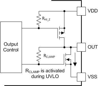
When the output stages of the driver are in an unbiased or UVLO condition, the driver outputs are held low by an active clamp circuit that limits the voltage rise on the driver outputs (illustrated in Figure 8-1). In this condition, the upper PMOS is resistively held off by RHi-Z while the lower NMOS gate is tied to the driver output through RCLAMP. In this configuration, the output is effectively clamped to the threshold voltage of the lower NMOS device, typically around 1.6V, regardless of whether bias power is available.
 Figure 8-1 Simplified Representation of Active Pull Down Feature
The VDD UVLO protection has a hysteresis feature (VVDD_HYS). This hysteresis prevents chatter when there is ground noise from the power supply. This also allows the device to accept small drops in bias voltage, which commonly occurs when the device starts switching and operating current consumption increases suddenly.
The inputs of the UCC2154x also has an internal under voltage lock out (UVLO) protection feature. The inputs cannot affect the outputs unless the supply voltage VCCI exceeds VVCCI_ON on start-up. The outputs are held low and cannot respond to inputs when the supply voltage VCCI drops below VVCCI_OFF after start-up. Like the UVLO for VDD, there is hystersis (VVCCI_HYS) to ensure stable operation.
| CONDITION | INPUTS | OUTPUTS | ||
|---|---|---|---|---|
| INA | INB | OUTA | OUTB | |
| VCCI-GND < VVCCI_ON during device start up | H | L | L | L |
| VCCI-GND < VVCCI_ON during device start up | L | H | L | L |
| VCCI-GND < VVCCI_ON during device start up | H | H | L | L |
| VCCI-GND < VVCCI_ON during device start up | L | L | L | L |
| VCCI-GND < VVCCI_OFF after device start up | H | L | L | L |
| VCCI-GND < VVCCI_OFF after device start up | L | H | L | L |
| VCCI-GND < VVCCI_OFF after device start up | H | H | L | L |
| VCCI-GND < VVCCI_OFF after device start up | L | L | L | L |
| CONDITION | INA | INB | OUTA | OUTB |
|---|---|---|---|---|
| INPUTS | OUTPUTS | |||
| VDD-VSS < VVDD_ON during device start up | H | L | L | L |
| VDD-VSS < VVDD_ON during device start up | L | H | L | L |
| VDD-VSS < VVDD_ON during device start up | H | H | L | L |
| VDD-VSS < VVDD_ON during device start up | L | L | L | L |
| VDD-VSS < VVDD_OFF after device start up | H | L | L | L |
| VDD-VSS < VVDD_OFF after device start up | L | H | L | L |
| VDD-VSS < VVDD_OFF after device start up | H | H | L | L |
| VDD-VSS < VVDD_OFF after device start up | L | L | L | L |