ZHCSKF2C February 2019 – January 2023 UCC21750
PRODUCTION DATA
- 1 特性
- 2 应用
- 3 说明
- 4 Revision History
- 5 Pin Configuration and Functions
-
6 Specifications
- 6.1 Absolute Maximum Ratings
- 6.2 ESD Ratings
- 6.3 Recommended Operating Conditions
- 6.4 Thermal Information
- 6.5 Power Ratings
- 6.6 Insulation Specifications
- 6.7 Safety Limiting Values
- 6.8 Electrical Characteristics
- 6.9 Safety-Related Certifications
- 6.10 Switching Characteristics
- 6.11 Insulation Characteristics Curves
- 6.12 Typical Characteristics
- 7 Parameter Measurement Information
-
8 Detailed Description
- 8.1 Overview
- 8.2 Functional Block Diagram
- 8.3
Feature Description
- 8.3.1 Power Supply
- 8.3.2 Driver Stage
- 8.3.3 VCC and VDD Undervoltage Lockout (UVLO)
- 8.3.4 Active Pulldown
- 8.3.5 Short Circuit Clamping
- 8.3.6 Internal Active Miller Clamp
- 8.3.7 Desaturation (DESAT) Protection
- 8.3.8 Soft Turn-Off
- 8.3.9 Fault (FLT, Reset, and Enable (RST/EN)
- 8.3.10 Isolated Analog to PWM Signal Function
- 8.4 Device Functional Modes
-
9 Applications and Implementation
- 9.1 Application Information
- 9.2
Typical Application
- 9.2.1 Design Requirements
- 9.2.2
Detailed Design Procedure
- 9.2.2.1 Input Filters for IN+, IN–, and RST/EN
- 9.2.2.2 PWM Interlock of IN+ and IN–
- 9.2.2.3 FLT, RDY, and RST/EN Pin Circuitry
- 9.2.2.4 RST/EN Pin Control
- 9.2.2.5 Turn-On and Turn-Off Gate Resistors
- 9.2.2.6 Overcurrent and Short Circuit Protection
- 9.2.2.7 Isolated Analog Signal Sensing
- 9.2.2.8 Higher Output Current Using an External Current Buffer
- 9.2.3 Application Curves
- 10Power Supply Recommendations
- 11Layout
- 12Device and Documentation Support
- 13Mechanical, Packaging, and Orderable Information
5 Pin Configuration and Functions
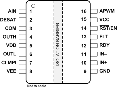
 Figure 5-1 UCC21750 DW SOIC (16) Top
View
Figure 5-1 UCC21750 DW SOIC (16) Top
ViewTable 5-1 Pin Functions
| PIN | I/O(1) | DESCRIPTION | |
|---|---|---|---|
| NAME | NO. | ||
| AIN | 1 | I | Isolated analog sensing input, parallel a small capacitor to COM for better noise immunity. Tie to COM if unused. |
| DESAT | 2 | I | Desaturation current protection input. Tie to COM if unused. |
| COM | 3 | P | Common ground reference, connecting to emitter pin for IGBT and source pin for SiC-MOSFET. |
| OUTH | 4 | O | Gate driver output pullup |
| VDD | 5 | P | Positive supply rail for gate drive voltage. Bypass with a >10-μF capacitor to COM to support specified gate driver source peak current capability. Place decoupling capacitor close to the pin. |
| OUTL | 6 | O | Gate driver output pull down |
| CLMPI | 7 | I | Internal active miller clamp, connecting this pin directly to the gate of the power transistor. Leave floating or tie to VEE if unused. |
| VEE | 8 | P | Negative supply rail for gate drive voltage. Bypass with a >10-μF capacitor to COM to support specified gate driver sink peak current capability. Place decoupling capacitor close to the pin. |
| GND | 9 | P | Input power supply and logic ground reference. |
| IN+ | 10 | I | Non-inverting gate driver control input. Tie to VCC if unused. |
| IN– | 11 | I | Inverting gate driver control input. Tie to GND if unused. |
| RDY | 12 | O | Power good for VCC-GND and VDD-COM. RDY is open drain configuration and can be paralleled with other RDY signals. |
| FLT | 13 | O | Active low fault alarm output upon over current or short circuit. FLT is in open drain configuration and can be paralleled with other faults. |
| RST/EN | 14 | I | The RST/EN serves two purposes: 1) Enable / shutdown of the output side. The FET is turned off by a regular turn-off, if terminal EN is set to low; 2) Resets the DESAT condition signaled on FLT pin. if terminal RST/EN is set to low for more than 1000ns. A reset of signal FLT is asserted at the rising edge of terminal RST/EN. For automatic RESET function, this pin only serves as an EN pin. Enable / shutdown of the output side. The FET is turned off by a regular turn-off, if terminal EN is set to low. |
| VCC | 15 | P | Input power supply from 3 V to 5.5 V. Bypass with a >1-μF capacitor to GND. Place decoupling capacitor close to the pin. |
| APWM | 16 | O | Isolated analog sensing PWM output. Leave floating if unused. |
(1) P = Power, G = Ground, I = Input,
O = Output