ZHCSMW1B October 2019 – March 2021 UCC23313-Q1
PRODUCTION DATA
- 1 特性
- 2 应用
- 3 说明
- 4 Revision History
- 5 Pin Configuration and Function
-
6 Specifications
- 6.1 Absolute Maximum Ratings
- 6.2 ESD Ratings
- 6.3 Recommended Operating Conditions
- 6.4 Thermal Information
- 6.5 Power Ratings
- 6.6 Insulation Specifications
- 6.7 Safety-Related Certifications
- 6.8 Safety Limiting Values
- 6.9 Electrical Characteristics
- 6.10 Switching Characteristics
- 6.11 Insulation Characteristics Curves
- 6.12 Typical Characteristics
- 7 Parameter Measurement Information
- 8 Detailed Description
- 9 Application and Implementation
- 10Power Supply Recommendations
- 11Layout
- 12Mechanical, Packaging, and Orderable Information
11.2 Layout Example
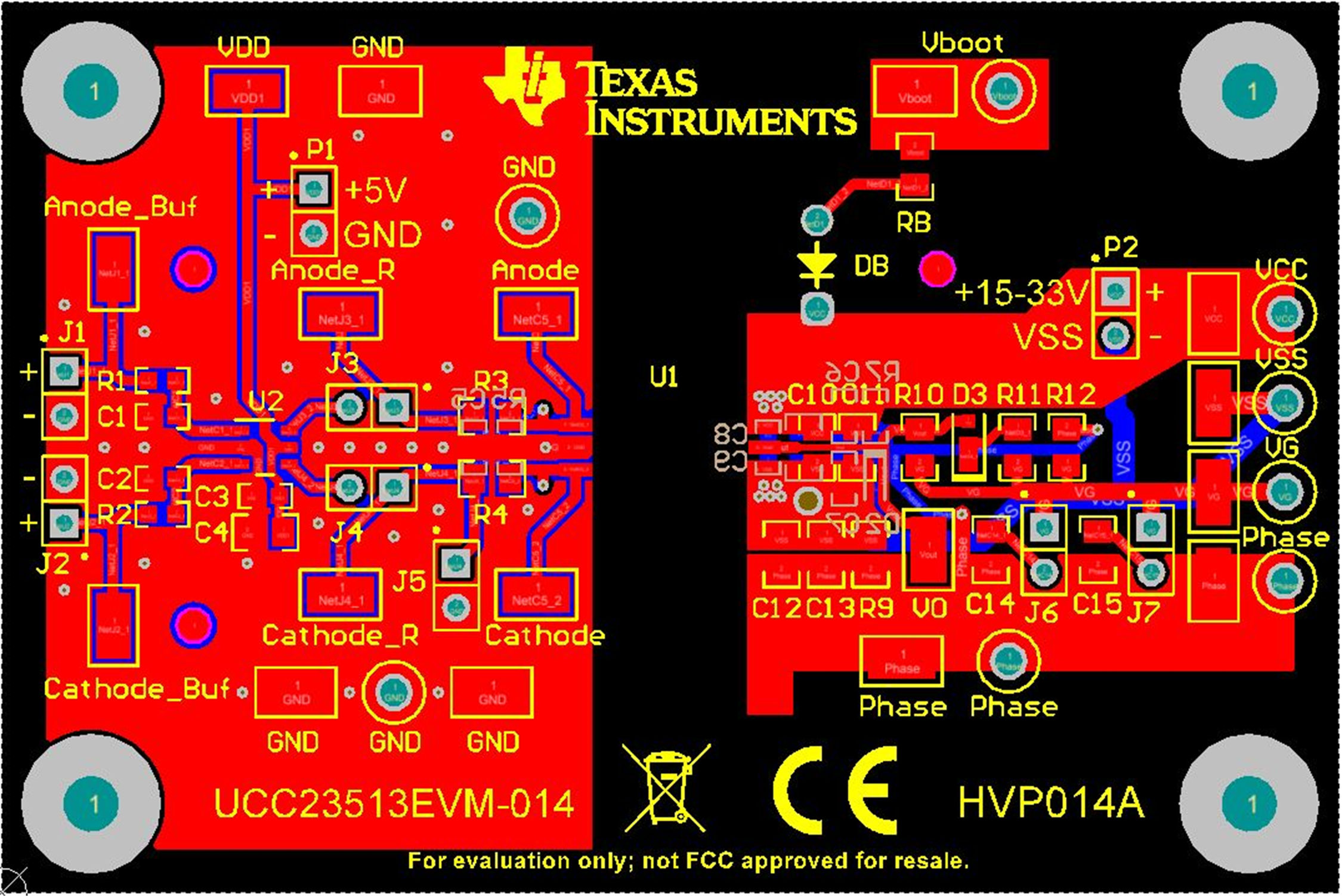
Figure 11-1 shows a PCB layout example with the signals and key components labeled.

No PCB traces or copper are located between the primary and secondary side, which ensures isolation performance.
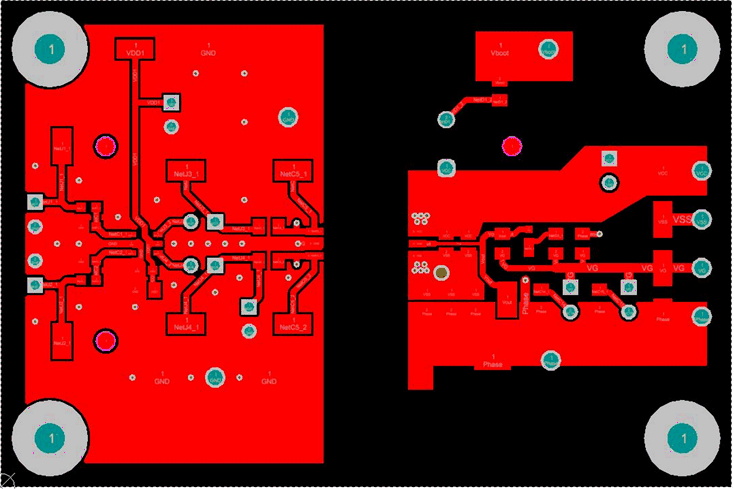
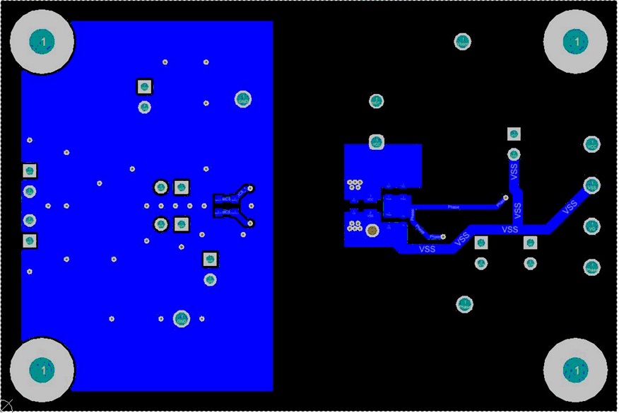
Figure 11-1 Layout ExampleFigure 11-2 and Figure 11-3 show the top and bottom layer traces and copper.
 Figure 11-2 Top-Layer Traces and Copper
 Figure 11-3 Bottom-Layer Traces and Copper (Flipped)
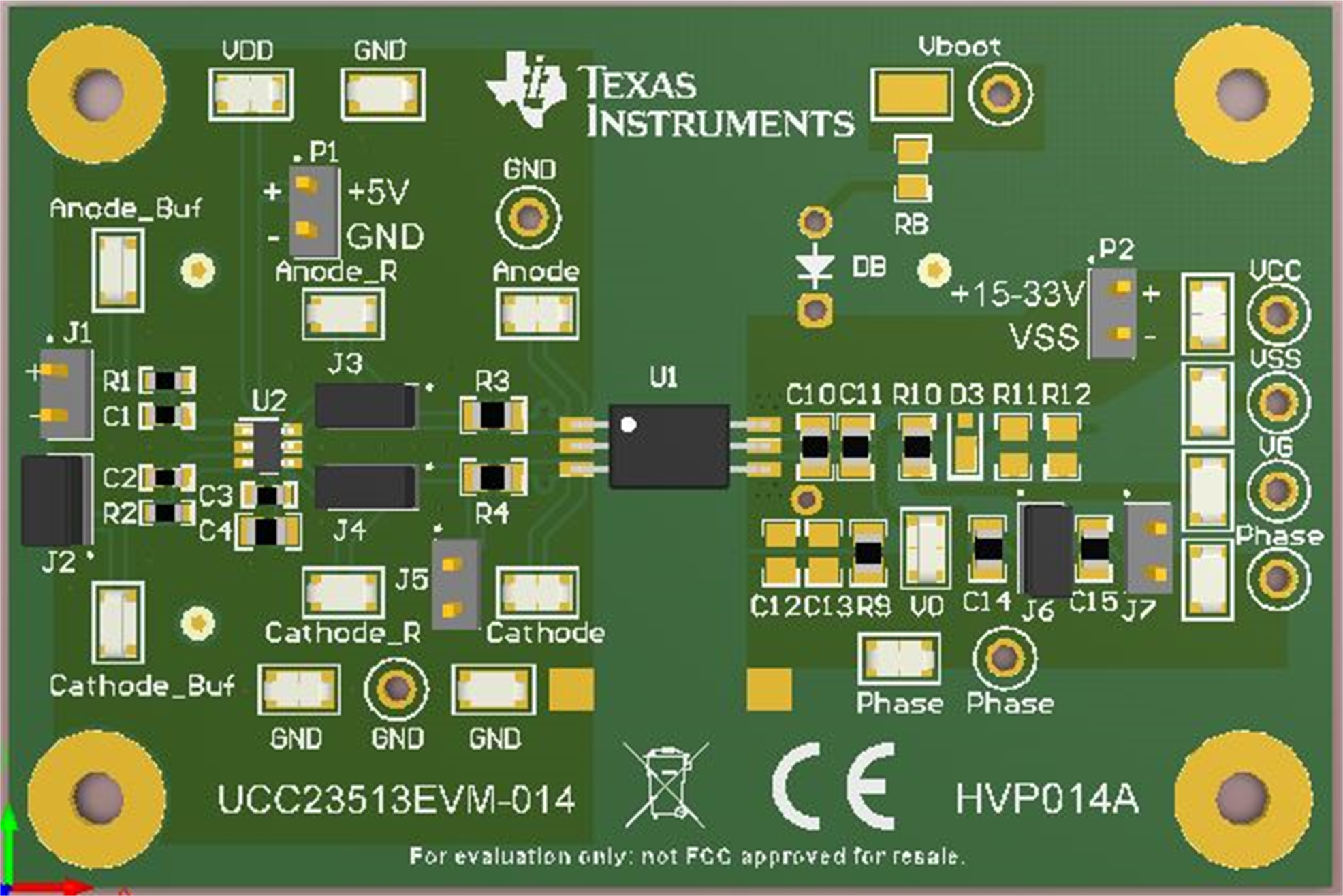
Figure 11-4 shows the 3D layout of the top view of the PCB.

The location of the PCB cutout between primary side and secondary sides ensures isolation performance.
Figure 11-4 3-D PCB View