ZHCSNL4A August 2020 – March 2021 UCC23511-Q1
PRODUCTION DATA
- 1 特性
- 2 应用
- 3 说明
- 4 Revision History
- 5 Pin Configuration and Function
-
6 Specifications
- 6.1 Absolute Maximum Ratings
- 6.2 ESD Ratings
- 6.3 Recommended Operating Conditions
- 6.4 Thermal Information
- 6.5 Power Ratings
- 6.6 Insulation Specifications
- 6.7 Safety-Related Certifications
- 6.8 Safety Limiting Values
- 6.9 Electrical Characteristics
- 6.10 Switching Characteristics
- 6.11 Insulation Characteristics Curves
- 6.12 Typical Characteristics
- 7 Parameter Measurement Information
- 8 Detailed Description
- 9 Device Functional Modes
- 10Application and Implementation
- 11Power Supply Recommendations
- 12Layout
- 13Mechanical, Packaging, and Orderable Information
10.2.2.1 Selecting the Input Resistor
The input resistor limits the current that flows into the e-diode when it is forward biased. The threshold current IFLH is 2.8 mA typ. The recommended operating range for the forward current is 7 mA to 16 mA (e-diode ON). All the electrical specifications are guaranteed in this range. The resistor should be selected such that for typical operating conditions, IF is 10 mA. Following are the list of factors that will affect the exact value of this current:
- Supply Voltage VSUP variation
- Manufacturer's tolerance for the resistor and variation due to temperature
- e-diode forward voltage drop variation (at IF=10 mA, VF= typ 2.1 V, min 1.8 V, max 2.4 V, with a temperature coefficient <1.35 mV/°C and dynamic impedance < 1 Ω)
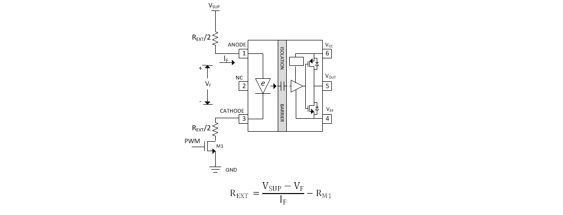
 Figure 10-2 Configuration 1: Driving the input stage of UCC23511-Q1 with a single NMOS and split resistors
Driving the input stage of UCC23511-Q1 using a single buffer is shown in Figure 10-3 and using 2 buffers is shown in Figure 10-4
 Figure 10-3 Configuration 2: Driving the input stage of UCC23511-Q1 with one Buffer and split resistors
 Figure 10-4 Configuration 3: Driving the input stage of UCC23511-Q1 with 2 buffers and split resistors
Table 10-2 shows the range of values for REXT for the 3 different configurations shown in Figure 10-2, Figure 10-3 and Figure 10-4.The assumptions used in deriving the range for REXT are as follows:
- Target forward current IF is 7mA min, 10mA typ and 16mA max
- e-diode forward voltage drop is 1.8V to 2.4V
- VSUP (Buffer supply voltage) is 5V with ±5% tolerance
- Manufacturer's tolerance for REXT is 1%
- NMOS resistance is 0.25Ω to 1.0Ω (for configuration 1)
- ROH(buffer output impedance in output "High" state) is 13Ω min, 18Ω typ and 22Ω max
- ROL(buffer output impedance in "Low" state) is 10Ω min, 14Ω typ and 17Ω max
| REXT Ω | |||
|---|---|---|---|
Configuration | Min | Typ | Max |
| Single NMOS and REXT | 218 | 290 | 331 |
| Single Buffer and REXT | 204 | 272 | 311 |
| Two Buffers and REXT | 194 | 259 | 294 |