ZHCSK29B september 2019 – october 2020 UCC23511
PRODUCTION DATA
- 1
- 1 特性
- 2 应用
- 3 说明
- 4 Revision History
- 5 Pin Configuration and Function
-
6 Specifications
- 6.1 Absolute Maximum Ratings
- 6.2 ESD Ratings
- 6.3 Recommended Operating Conditions
- 6.4 Thermal Information
- 6.5 Power Ratings
- 6.6 Insulation Specifications
- 6.7 Safety-Related Certifications
- 6.8 Safety Limiting Values
- 6.9 Electrical Characteristics
- 6.10 Switching Characteristics
- 6.11 Insulation Characteristics Curves
- 6.12 Typical Characteristics
- 7 Parameter Measurement Information
- 8 Detailed Description
- 9 Application and Implementation
- 10Power Supply Recommendations
- 11Layout
- 12Mechanical, Packaging, and Orderable Information
8.3.2 Input Stage
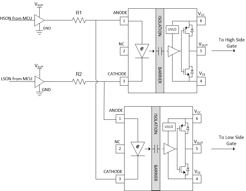
The input stage of UCC23511 is simply the e-diode and therefore has an Anode (Pin 1) and a Cathode (Pin 3). Pin 2 has no internal connection and can be left open or connected to ground. The input stage does not have a power and ground pin. When the e-diode is forward biased by applying a positive voltage to the Anode with respect to the Cathode, a forward current IF flows into the e-diode. The forward voltage drop across the e-diode is 2.1V (typ). An external resistor should be used to limit the forward current. The recommended range for the forward current is 7mA to 16mA. When IF exceeds the threshold current IFLH(2.8mA typ.) a high frequency signal is transmitted across the isolation barrier through the high voltage SiO2 capacitors. The HF signal is detected by the receiver and VOUT is driven high. See Section 9.2.2.1 for information on selecting the input resistor. The dynamic impedance of the e-diode is very small(<1.0Ω) and the temperature coefficient of the e-diode forward voltage drop is <1.35mV/°C. This leads to excellent stability of the forward current IF across all operating conditions. If the Anode voltage drops below VF_HL (0.9V), or reverse biased, the gate driver output is driven low. The reverse breakdown voltage of the e-diode is >15V. So for normal operation, a reverse bias of up to 13V is allowed. The large reverse breakdown voltage of the e-diode enables UCC23511 to be operated in interlock architecture (see example in Figure 8-3) where VSUP can be as high as 12V. The system designer has the flexibility to choose a 3.3V, 5.0V or up to 12V PWM signal source to drive the input stage of UCC23511 using an appropriate input resistor. The example shows two gate drivers driving a set of IGBTs. The inputs of the gate drivers are connected as shown and driven by two buffers that are controlled by the MCU. Interlock architecture prevents both the e-diodes from being "ON" at the same time, preventing shoot through in the IGBTs. It also ensures that if both PWM signals are erroneously stuck high (or low) simultaneously, both gate driver outputs will be driven low.
 Figure 8-3 Interlock