ZHCSDK6A March   2015  – March 2015 UCC24630

PRODUCTION DATA.  

  1. 特性
  2. 应用
  3. 说明
  4. 修订历史记录
  5. Pin Configuration and Functions
  6. Specifications
    1. 6.1 Absolute Maximum Ratings
    2. 6.2 ESD Ratings
    3. 6.3 Recommended Operating Conditions
    4. 6.4 Thermal Information
    5. 6.5 Electrical Characteristics
    6. 6.6 Timing Requirements
    7. 6.7 Typical Characteristics
  7. Detailed Description
    1. 7.1 Overview
    2. 7.2 Functional Block Diagram
    3. 7.3 Feature Description
      1. 7.3.1 Start Up and UVLO
      2. 7.3.2 Volt-Sec SR Driver On-Time Control
      3. 7.3.3 CCM Dead Time
      4. 7.3.4 Standby Operation
      5. 7.3.5 Pin Fault Protection
        1. 7.3.5.1 VPC Pin Overvoltage
        2. 7.3.5.2 VPC Pin Open
        3. 7.3.5.3 VSC Pin Open
        4. 7.3.5.4 TBLK Pin Open
        5. 7.3.5.5 VPC and VSC Short to Ground
        6. 7.3.5.6 TBLK Pin Short to Ground
    4. 7.4 Device Functional Modes
      1. 7.4.1 Start-Up
      2. 7.4.2 Normal Operation
      3. 7.4.3 Standby Operation
      4. 7.4.4 Conditions to Stop Operation
  8. Application and Implementation
    1. 8.1 Application Information
    2. 8.2 Typical Application
      1. 8.2.1 AC-to-DC Adapter, 19.5 V, 65 W
      2. 8.2.2 Design Requirements
      3. 8.2.3 Calculation of Component Values
        1. 8.2.3.1 VPC Input
        2. 8.2.3.2 VSC Input
        3. 8.2.3.3 TBLK Input
      4. 8.2.4 Application Curves
    3. 8.3 Do's and Don'ts
  9. Power Supply Recommendations
  10. 10Layout
    1. 10.1 Layout Guidelines
      1. 10.1.1 VDD Pin
      2. 10.1.2 VPC Pin
      3. 10.1.3 VSC Pin
      4. 10.1.4 GND Pin
      5. 10.1.5 TBLK Pin
      6. 10.1.6 DRV Pin
    2. 10.2 Layout Example
  11. 11器件和文档支持
    1. 11.1 器件支持
      1. 11.1.1 器件命名规则
        1. 11.1.1.1 术语定义
    2. 11.2 商标
    3. 11.3 静电放电警告
    4. 11.4 Glossary
  12. 12机械、封装和可订购信息

封装选项

机械数据 (封装 | 引脚)
散热焊盘机械数据 (封装 | 引脚)
订购信息

5 Pin Configuration and Functions

DBV Package
6-Pin SOT23
Top View
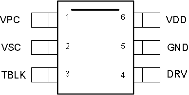
UCC24630 pin_lusc82.gif

Pin Functions

PIN I/O(1) DESCRIPTION
NAME NO.
DRV 4 O DRiVe is an output used to drive the gate of an external synchronous rectifier N-channel MOSFET switching transistor, with source pin connected to GND.
GND 5 G The GrouND pin is both the reference pin for the controller and the low-side return for the drive output. Special care should be taken to return all AC decoupling capacitors as close as possible to this pin and avoid any common trace length with analog signal return paths.
TBLK 3 Time BLanK pin is used to select the blanking time of the VPC rising edge. A programmable range from 200 ns to 1 µs is available to prevent false detection of the primary on-time due to ringing during DCM operation.
VDD 6 P VDD is the bias supply input pin to the controller. A carefully placed bypass capacitor to GND is required on this pin.
VPC 1 I The Voltage during Primary Conduction pin is connected to a resistor divider from the SR MOSFET drain. This pin determines a sample of the primary-side MOSFET volt seconds during the primary on-time. This voltage programs a voltage controlled current source for the internal VPC ramp charging current.
VSC 2 I The Voltage during Secondary Conduction pin is connected to a resistor divider from the power-supply output. This pin determines a sample of the secondary-side output voltage used to determine SR MOSFET conduction time. This voltage programs a voltage controlled current source for the internal VSC ramp charging current.
(1) P = Power, G = Ground, I = Input, O = Output, I/O = Input/Output