ZHCSES5A March 2016 – March 2016 UCC24636
PRODUCTION DATA.
- 1 特性
- 2 应用
- 3 说明
- 4 修订历史记录
- 5 Device Comparison Table
- 6 Pin Configuration and Functions
- 7 Specifications
- 8 Detailed Description
- 9 Application and Implementation
- 10Power Supply Recommendations
- 11Layout
- 12器件和文档支持
- 13机械、封装和可订购信息
11 Layout
11.1 Layout Guidelines
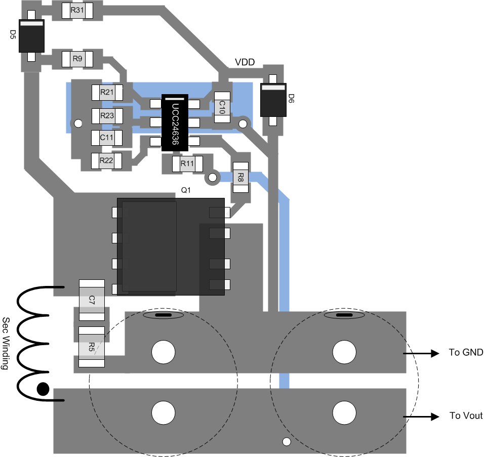
In general, try to keep all high current loops as short as possible. Keep all high current/high frequency traces away from other traces in the design. If necessary, high-frequency/high-current traces should be perpendicular to signal traces, not parallel to them. Shielding signal traces with ground traces can help reduce noise pick up. Always consider appropriate clearances between the high-voltage connections and any low-voltage nets.
11.1.1 VDD Pin
The VDD pin must be decoupled to GND with good quality, low ESR, low ESL ceramic bypass capacitors with short traces to the VDD and GND pins. To eliminate high-frequency ripple current in the SR control circuit, it is recommended to place a small value resistance of 2.2 Ω to 10 Ω between VDD and the converter output voltage.
11.1.2 VPC Pin
The trace between the resistor divider and the VPC pin should be as short as possible to reduce/eliminate possible noise coupling. The lower resistor of the resistor divider network connected to the VPC pin should be returned to GND with short traces. Avoid adding any significant external capacitance to the VPC pin so that there is no delay of signal. If filtering is necessary a recommended maximum capacitance is 15 pF with a lower resistor divider network value of 10 kΩ. Avoid high dV/dt traces close to the VPC pin and connection trace such as the SR MOSFET drain and DRV output.
11.1.3 VSC Pin
The trace between the resistor divider and the VSC pin should be as short as possible to reduce/eliminate possible noise coupling. The lower resistor of the resistor divider network connected to the VSC pin should be returned to GND with short traces. External capacitance can be added to the VSC pin for noise filtering. The maximum capacitance consideration is a time constant of the capacitor and the resistor divider resistance that is less than 1/4 the minimum rise time of the converter output during startup. Avoid high dV/dt traces close to the VSC pin and connection trace such as the SR MOSFET drain and DRV output.
11.1.4 GND Pin
The GND pin is the power and signal ground connection for the controller. The effectiveness of the filter capacitors on the signal pins depends upon the integrity of the ground return. Place all decoupling capacitors as close as possible to the device pins with short traces. The device ground and power ground should meet at the output bulk capacitor’s return. Try to ensure that high frequency/high current from the power stage does not go through the signal ground.
11.1.5 TBLK Pin
The programming resistor is placed on TBLK to GND, with short traces. The value may have to be adjusted based on the time delay required. Avoid high dV/dt traces close to the TBLK pin and connection trace such as the SR MOSFET drain and DRV output.
11.1.6 DRV Pin
The track connected to DRV carries high dv/dt signals. Minimize noise pickup by routing the trace to this pin as far away as possible from tracks connected to the device signal inputs, VPC, VSC, and TBLK.
11.2 Layout Example
