ZHCSES5A March 2016 – March 2016 UCC24636
PRODUCTION DATA.
- 1 特性
- 2 应用
- 3 说明
- 4 修订历史记录
- 5 Device Comparison Table
- 6 Pin Configuration and Functions
- 7 Specifications
- 8 Detailed Description
- 9 Application and Implementation
- 10Power Supply Recommendations
- 11Layout
- 12器件和文档支持
- 13机械、封装和可订购信息
7 Specifications
7.1 Absolute Maximum Ratings
over operating free-air temperature range (unless otherwise noted)(1)| MIN | MAX | UNIT | |||
|---|---|---|---|---|---|
| VVDD | Bias supply voltage, VDD | –0.3 | 30 | V | |
| IDRV | Continuous gate current sink, DRV | 50 | mA | ||
| IDRV | Continuous gate current source, DRV | –50 | mA | ||
| IVPC | Peak VPC pin current | –1.2 | mA | ||
| VDRV | Gate drive voltage at DRV | –0.3 | Self-limiting | V | |
| VVPC, VVSC | Voltage range, VPC, VSC | –0.3 | 4.5 | V | |
| TJ | Operating junction temperature range | –55 | 150 | °C | |
| TL | Lead temperature 0.6 mm from case for 10 seconds | 260 | °C | ||
| Tstg | Storage temperature | –65 | 150 | °C | |
(1) Stresses beyond those listed under Absolute Maximum Ratings may cause permanent damage to the device. These are stress ratings only, which do not imply functional operation of the device at these or any other conditions beyond those indicated under Recommended Operating Conditions. Exposure to absolute-maximum-rated conditions for extended periods may affect device reliability.
7.2 ESD Ratings
| VALUE | UNIT | |||
|---|---|---|---|---|
| V(ESD) | Electrostatic discharge | Human-body model (HBM), per ANSI/ESDA/JEDEC JS-001(1) | ±2000 | V |
| Charged-device model (CDM), per JEDEC specification JESD22-C101(2) | ±500 | |||
(1) JEDEC document JEP155 states that 2000-V HBM allows safe manufacturing with a standard ESD control process. Pins listed as ±2000 V may actually have higher performance.
(2) JEDEC document JEP157 states that 500-V CDM allows safe manufacturing with a standard ESD control process. Pins listed as ±500 V may actually have higher performance.
7.3 Recommended Operating Conditions
over operating free-air temperature range (unless otherwise noted)| MIN | MAX | UNIT | ||
|---|---|---|---|---|
| VVDD | Bias supply operating voltage | 3.75 | 28 | V |
| CVDD | VDD bypass capacitor | 0.22 | µF | |
| TJ | Operating junction temperature | -40 | 125 | °C |
| VVPC, VVSC | Operating range | –0.3 | 2.2 | V |
7.4 Thermal Information
| THERMAL METRIC(1) | UCC24636 | UNIT | |
|---|---|---|---|
| DBV (SOT23) | |||
| 6 PINS | |||
| RθJA | Junction-to-ambient thermal resistance | 180 | °C/W |
| RθJC(top) | Junction-to-case (top) thermal resistance | 71.2 | °C/W |
| RθJB | Junction-to-board thermal resistance | 44 | °C/W |
| ψJT | Junction-to-top characterization parameter | 5.1 | °C/W |
| ψJB | Junction-to-board characterization parameter | 13.8 | °C/W |
(1) For more information about traditional and new thermal metrics, see the Semiconductor and IC Package Thermal Metrics application report, SPRA953.
7.5 Electrical Characteristics
over operating free-air temperature, VDD = 12 V, TA = –40°C to 125°C, TA = TJ (unless otherwise noted)| PARAMETER | TEST CONDITION | MIN | TYP | MAX | UNIT | |
|---|---|---|---|---|---|---|
| SUPPLY INPUT | ||||||
| IRUN | Supply current, run | IDRV = 0, run state, FSW = 0 kHz | 0.9 | 1.2 | mA | |
| ISTBY | Supply current, standby | IDRV = 0, standby mode | 110 | 160 | µA | |
| UNDER-VOLTAGE LOCKOUT | ||||||
| VVDD(on) | VDD turn-on threshold | VVDD low to high | 3.9 | 4 | 4.3 | V |
| VVDD(off) | VDD turn-off threshold | VVDD high to low | 3.3 | 3.6 | 3.7 | V |
| DRV | ||||||
| RDRVLS | DRV low-side drive resistance | IDRV = 100 mA | 1 | 2 | Ω | |
| VDRVST | DRV pull down in start-up | VDD= 0 to 2 V, IDRV= 10 µA | 0.95 | V | ||
| VDRCL | DRV clamp voltage | VVDD = 30 V | 11 | 13 | 15 | V |
| VPMOS | Disable PMOS high-side drive | VDD voltage to disable rail-to-rail drive, VDD rising | 9.3 | 10 | 10.5 | V |
| VPMOS-HYS | PMOS enable hysteresis | VDD voltage hysteresis to enable rail to rail drive, VDD falling | 0.75 | 1 | 1.25 | V |
| VDRHI | DRV pull-up high voltage | VVDD = 5 V, IDRV = 15 mA | 4.6 | 4.75 | 5 | V |
| VSC INPUT | ||||||
| VVSCEN | SR enable voltage | VVSC > VVSCEN, VVSC rising | 250 | 300 | 340 | mV |
| VVSC-HYS | SR enable hysteresis | VVSC falling | 50 | mV | ||
| VVSCDIS | SR disable voltage | 220 | 250 | 280 | mV | |
| IVSC | Input bias current | VVSC = 2 V | –0.25 | 0 | 0.4 | µA |
| VPC INPUT | ||||||
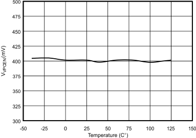
| VVPCEN | SR enable voltage | VVPCEN < VVPC | 345 | 400 | 450 | mV |
| VVPCDIS | VPC threshold to disable SR | VVPC > VVPCDIS | 2.6 | 2.85 | 3.1 | V |
| VVPC-TH | Threshold of VVPC rising edge | VVPC = 0.95 V, VVPC-TH = 0.85 x VVPC previous cycle | 0.76 | 0.808 | 0.86 | V |
| VVPC-TH-CLP | Clamp threshold of VVPC rising edge | VVPC = 2 V | 0.9 | 1 | 1.1 | V |
| IVPC | Input bias current | VVPC = 2 V | –0.25 | 0 | 0.4 | µA |
| CURRENT EMULATOR | ||||||
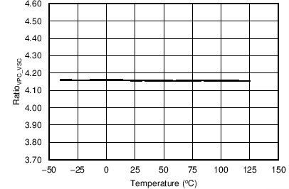
| RatioVPC_VSC | KVPC/KVSC | VVPC = 1.25 V, tVPC = 1 µs, VVSC = 1.25 V |
3.97 | 4.17 | 4.35 | |
| VVPC = 1.25 V, tVPC = 5 µs, VVSC = 1.25 V |
3.95 | 4.17 | 4.37 | |||
| VVPC = 2 V, tVPC = 1 µs, VVSC = 1.25 V |
3.85 | 4.09 | 4.26 | |||
| VVPC = 1.25 V, tVPC = 1 µs, VVSC = 0.45 V |
3.85 | 4.07 | 4.28 | |||
| STANDBY OPERATION | ||||||
| nENTO | Number of switching cycles to enter standby operation during tENTO | 64 | ||||
| nEN | Number of switching cycles to exit standby operation during tEN(1) | 32 | ||||
| OVER TEMPERATURE PROTECTION | ||||||
| T(STOP) | Thermal shutdown temperature | Internal junction temperature | 165 | °C | ||
(1) The device exits standby operation as soon as nEN occurs within tEN.
7.6 Timing Requirements
over operating free-air temperature range, VDD = 12 V, TA = –40°C to 125°C, TA = TJ (unless otherwise noted)| PARAMETER | TEST CONDITION | MIN | TYP | MAX | UNIT | |
|---|---|---|---|---|---|---|
| DRV | ||||||
| tR | DRV high-side rise time | VVDD = 12 V, CL = 3.3 nF, VDRV = 2 V to 8 V | 27 | 54 | ns | |
| VVDD = 5 V, CL = 3.3 nF, VDRV = 1 V to 4 V | 50 | 100 | ||||
| tF | DRV low-side fall time | VVDD = 12 V, CL = 3.3 nF, VDRV = 8 V to 2 V | 20 | 54 | ns | |
| VVDD = 5 V, CL = 3.3 nF, VDRV = 4 V to 1 V | 15 | 50 | ||||
| tDRVON | Propagation delay to DRV High | VVPC = 1 V to –0.05 V falling to DRV high, VVDD = 12 V, VDRV = 0 V to 2 V |
80 | 160 | ns | |
| tDRVOFF | Propagation delay to DRV Low | Test mode | 65 | 95 | ns | |
| VPC INPUT | ||||||
| tVPC-SPL | VPC sampling time window | 81 | 100 | 125 | ns | |
| tVPC-BLK | Minimum VPC pulse for SR DRV operation | RTBLK = 5 kΩ | 169 | 203 | 239 | ns |
| RTBLK = 50 kΩ | 0.85 | 1.01 | 1.18 | µs | ||
| SR ON CONTROL | ||||||
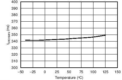
| tSRONMIN | SR minimum on time after VPC falling. | 300 | 350 | 425 | ns | |
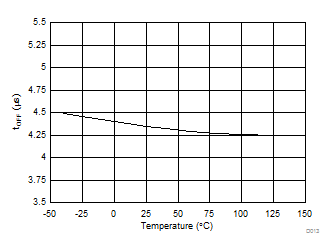
| tOFF | SR off blanking time from DRV falling. | 3.96 | 4.35 | 4.75 | us | |
| STANDBY OPERATION | ||||||
| tENTO | Time to disable SR operation, enter standby | Time to disable DRV | 11.5 | 12.8 | 14.1 | ms |
| tEN | Time to enable SR operation, exit standby operation | Time to enable DRV(1) | 2.3 | 2.56 | 2.82 | ms |
(1) The device exits standby operation as soon as nEN occurs within tEN.
7.7 Typical Characteristics
VVDD = 12 V, TJ = 25°C, unless otherwise noted.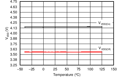
| VVPC = 1.25 V | tVPC = 1 µs | VVSC = 1.25 V |
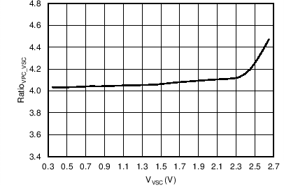
| VVPC = 1.25 V | tVPC = 2 µs |
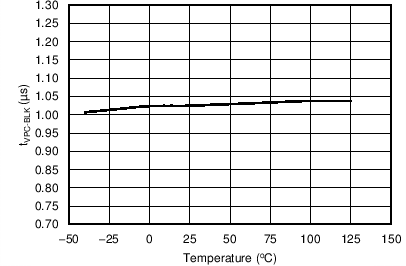
| RTBLK = 50 kΩ |
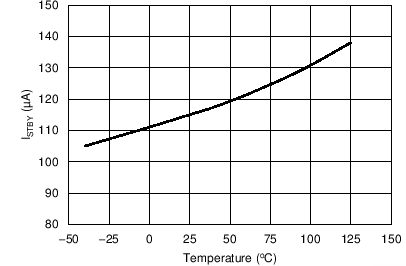
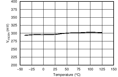
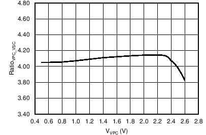
| VVSC = 1.25 V | tVPC × VVPC = 3 V-µs |
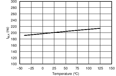
| RTBLK = 5 kΩ |
