ZHCSDB6 February 2015 UCC24650
PRODUCTION DATA.
6 Specifications
6.1 Absolute Maximum Ratings
over operating free-air temperature range (unless otherwise noted)(1)| MIN | MAX | UNIT | ||
|---|---|---|---|---|
| Input voltage | VCC | –0.5 | 30 | V |
| WAKE | (2) | 230 | ||
| ENS | –0.5 | 7 | ||
| Source current | WAKE | 10 | mA | |
| ENS | 1 | |||
| Sink current | WAKE | Self-limiting | mA | |
| ENS | 0.5 | |||
| TJ | Operating junction temperature | –55 | 150 | °C |
| Tlead | Lead temperature 0.6 mm from case for 10 s | 260 | ||
| Tstg | Storage temperature | –65 | 150 | |
(1) Stresses beyond those listed under Absolute Maximum Ratings may cause permanent damage to the device. These are stress ratings only, which do not imply functional operation of the device at these or any other conditions beyond those indicated under Recommended Operating Conditions. Exposure to absolute-maximum-rated conditions for extended periods may affect device reliability.
(2) The WAKE pin is normally brought below GND by a system-level rectifier. A negative voltage level is not of concern provided that the absolute maximum source current limit is observed.
6.2 ESD Ratings
| VALUE | UNIT | ||||
|---|---|---|---|---|---|
| V(ESD) | Electrostatic discharge | Human body model (HBM), per ANSI/ESDA/JEDEC JS-001(1) | All pins except pin 5 | ±2000 | V |
| Pin 5 | ±1500 | ||||
| Charged-device model (CDM), per JEDEC specification JESD22-C101(2) | All pins | ±1000 | |||
(1) JEDEC document JEP155 states that 500-V HBM allows safe manufacturing with a standard ESD control process.
(2) JEDEC document JEP157 states that 250-V CDM allows safe manufacturing with a standard ESD control process.
6.3 Recommended Operating Conditions
over operating free-air temperature range (unless otherwise noted)| MIN | NOM | MAX | UNIT | ||
|---|---|---|---|---|---|
| VVDD | Bias-supply operating voltage | 4.5 | 28 | V | |
| VWAKE | WAKE pin voltage | 200 | V | ||
| VENS | ENS pin voltage(1) | 0 | 6 | V | |
| tPCD | Power cycle detect interval | 40 | ms | ||
| TJ | Operating junction temperature range | –40 | 125 | °C | |
(1) The UCC24650 enters a manufacturing test mode when ENS is driven below 0 V and normal operation is impaired during this condition. If the ENS function is not used, connect ENS to GND to avoid triggering the test mode by noise on an open pin.
6.4 Thermal Information
| THERMAL METRIC(1) | UCC24650 | UNIT | |
|---|---|---|---|
| DBV | |||
| 5 PINS | |||
| RθJA | Junction-to-ambient thermal resistance | 200.2 | °C/W |
| RθJC(top) | Junction-to-case (top) thermal resistance | 125.5 | |
| RθJB | Junction-to-board thermal resistance | 35.8 | |
| ψJT | Junction-to-top characterization parameter | 18.4 | |
| ψJB | Junction-to-board characterization parameter | 35.0 | |
(1) For more information about traditional and new thermal metrics, see the IC Package Thermal Metrics application report, SPRA953.
6.5 Electrical Characteristics
over operating free-air temperature range, VVDD = 5 V, VWAKE = 5 V, –40°C ≤ TA ≤ 125°C, TJ = TA, (unless otherwise noted)| PARAMETER | TEST CONDITIONS | MIN | TYP | MAX | UNIT | |
|---|---|---|---|---|---|---|
| SUPPLY INPUT | ||||||
| IVDD28 | Supply current | VVDD = 28 V, VWAKE = 28 V | 43 | 63 | 83 | µA |
| IVDD5 | Supply current | VVDD = 5 V, VWAKE = 5 V | 30 | 41 | 52 | µA |
| VUVLO(on) | UVLO turn-on voltage at VDD | VVDD rising threshold | 3.6 | 4.0 | 4.4 | V |
| VUVLO(hyst) | UVLO hysteresis | VUVLO(on) – VVDD falling threshold | 170 | 250 | 330 | mV |
| WAKE INPUT | ||||||
| VPCD | PCD voltage threshold | VWAKE high to low | 10 | 55 | 100 | mV |
| IWAKE | Input bias current, out of pin | VWAKE = 0 V | 0 | 0.1 | µA | |
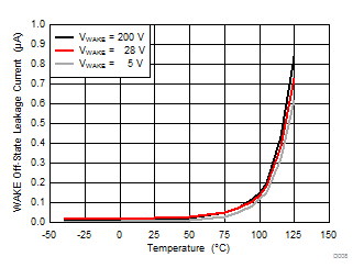
| IWAKE(lkg)cool(1) | Input leakage current, into pin, cool | VWAKE = 200 V, -40°C ≤ TJ ≤ 85°C | 0 | 0.2 | µA | |
| IWAKE(lkg)hot(1) | Input leakage current, into pin, hot | VWAKE = 200 V, 85°C ≤ TJ ≤ 125°C | 0 | 3 | µA | |
| WAKE-UP FUNCTION | ||||||
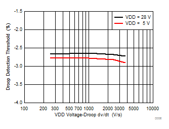
| ΔVVDD5(cool)(1)(2) | Droop threshold, over cool temperature range | Drop in VVDD following a power-cycle detect by 40 ms, VVDD falling from 5 V, dv/dt = –250 V/s, –40°C ≤ TJ ≤ 85°C | –2.30% | –2.77% | –3.20% | |
| ΔVVDD5(hot)(1)(2) | Wake-up droop threshold, over hot temperature range | Drop in VVDD following a power-cycle detect by 40 ms, VVDD falling from 5 V, dv/dt = –250 V/s, 85°C ≤ TJ ≤ 125°C | –1.50% | –2.74% | –4.0% | |
| ΔVVDD28(1)(2) | Wake-up droop threshold, over full temperature range | Drop in VVDD following a power-cycle detect by 40 ms, VVDD falling from 28 V, dv/dt = –250 V/s | –2.3% | –2.7% | –3.2% | |
| IWAKE(on)25 | Wake-up drive current, room temperature | VWAKE = 4 V, TJ = 25°C | 20 | 27 | mA | |
| IWAKELMT | Wake-up current limit | VVDD = 28 V, VWAKE = 28 V | 35 | 48 | 60 | mA |
| ENABLE SECONDARY CIRCUIT FUNCTION | ||||||
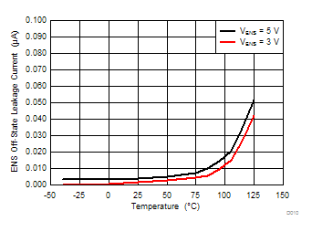
| IENS(lkg) | ENS switch leakage current | VENS = 5 V, off-state | 0 | 0.1 | µA | |
| RENS(RDS(on)) | ENS switch on-resistance | IENS = 100 µA, on-state | 1.3 | 2.7 | 5.0 | kΩ |
(1) Device parameter characterized during development. Not production tested, except at 25°C.
(2) For droop threshold at higher dv/dt, see Typical Characteristics.
6.6 Timing Requirements
over operating free-air temperature range, VVDD = 5 V, VWAKE = 5 V, –40°C ≤ TA ≤ 125°C, TJ = TA, (unless otherwise noted)| MIN | NOM | MAX | UNIT | ||
|---|---|---|---|---|---|
| tPCD(min) | PCD minimum time for VWAKE < VPCD | 350 | 500 | 650 | ns |
| tSW(max) | PCD maximum period for ΔVVDD | 40 | ms | ||
6.7 Switching Characteristics
over operating free-air temperature range, VVDD = 5 V, VWAKE = 5 V, –40°C ≤ TA ≤ 125°C, TJ = TA, (unless otherwise noted)| PARAMETER | TEST CONDITIONS | MIN | TYP | MAX | UNIT | |
|---|---|---|---|---|---|---|
| WAKE-UP FUNCTION | ||||||
| tWAKE | Wake-up pulse width | ΔVVDD ≥ –5% after PCD | 0.7 | 1 | 1.3 | µs |
| tWAKE(rep) | Wake-up repeat period | ΔVVDD ≥ –5% after PCD | 21 | 30 | 39 | µs |
| ENABLE SECONDARY CIRCUIT FUNCTION | ||||||
| tENS(1) | Qualifying tSW to enable secondary circuit | WAKE input toggling | 40 | 57 | 74 | µs |
| NENS | Cumulative cycles to enable secondary circuit | tSW < tENS | 32 | cycles | ||
| tDISS(1) | Qualifying tSW to disable secondary circuit | WAKE input toggling | 124 | 177 | 230 | µs |
| NDISS | Consecutive cycles to disable secondary circuit | tSW > tDISS | 63 | cycles | ||
(1) By design, the ratio of tENS to tDISS remains within ±10% of typical, over all conditions. Not production tested.
6.8 Typical Characteristics
VVDD = 5 V, VWAKE = 5 V, TA = 25°C, TJ = TA, (unless otherwise noted)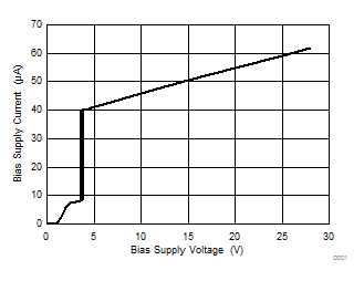
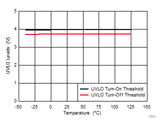
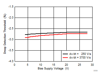
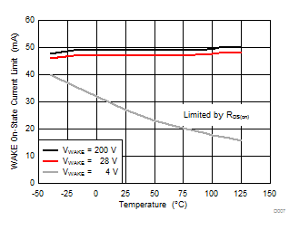
| No external series resistance | ||
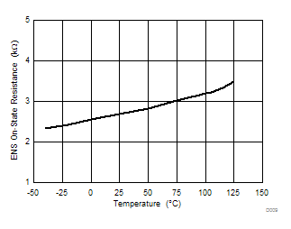
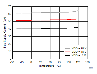
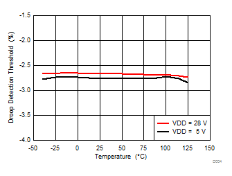
| dv/dt = 250 V/s | ||
