ZHCSJY8E june 2019 – february 2021 UCC256402 , UCC256403 , UCC256404
PRODUCTION DATA
- 1 特性
- 2 应用
- 3 说明
- 4 Revision History
- 5 Pin Configuration and Functions
- 6 Specifications
-
7 Detailed Description
- 7.1 Overview
- 7.2 Functional Block Diagram
- 7.3 Feature Description
- 7.4
Device Functional Modes
- 7.4.1 High Voltage Start-Up
- 7.4.2 X-Capacitor Discharge
- 7.4.3 Burst Mode Control
- 7.4.4
System State Machine
-
Application and Implementation
- 8.1 Application Information
- 8.2
Typical Application
- 8.2.1 Design Requirements
- 8.2.2
Detailed Design Procedure
- 8.2.2.1 LLC Power Stage Requirements
- 8.2.2.2 LLC Gain Range
- 8.2.2.3 Select Ln and Qe
- 8.2.2.4 Determine Equivalent Load Resistance
- 8.2.2.5 Determine Component Parameters for LLC Resonant Circuit
- 8.2.2.6 LLC Primary-Side Currents
- 8.2.2.7 LLC Secondary-Side Currents
- 8.2.2.8 LLC Transformer
- 8.2.2.9 LLC Resonant Inductor
- 8.2.2.10 LLC Resonant Capacitor
- 8.2.2.11 LLC Primary-Side MOSFETs
- 8.2.2.12 LLC Rectifier Diodes
- 8.2.2.13 LLC Output Capacitors
- 8.2.2.14 HV Pin Series Resistors
- 8.2.2.15 BLK Pin Voltage Divider
- 8.2.2.16 ISNS Pin Differentiator
- 8.2.2.17 VCR Pin Capacitor Divider
- 8.2.2.18 BW Pin Voltage Divider
- 8.2.2.19 Soft Start and Burst Mode Programming
- 8.2.3 Application Curves
-
Application and Implementation
- 8 Power Supply Recommendations
- 9 Layout
- 10Device and Documentation Support
7.3.9.1 ZCS Region Prevention
The capacitive region is an LLC operating region in which the voltage gain increases when the switching frequency increases. It is also called the ZCS region. Capacitive mode operation should be avoided for two reasons:
- The feedback loop becomes positive feedback in the capacitive region
- The MOSFET may be damaged because of body diode reverse recovery
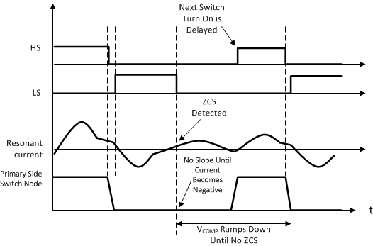
The capacitive region detection is done by checking the resonant current polarity at HSON or LSON falling edge. If the resonant current is positive at LSON falling edge, or negative at HSON falling edge, the ZCS signal in the waveform generator is turned high. The ZCS signal stays high until ZCS is cleared at the next HSON or LSON falling edge.
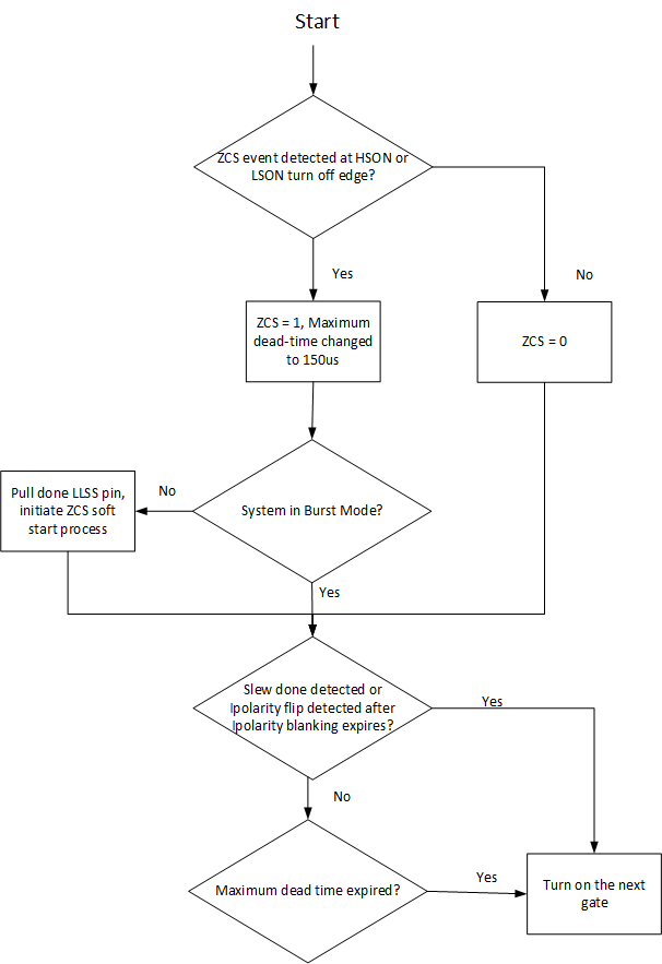
If ZCS is detected, the next gate will be turned on at the next IPolarity flip event when the resonant current becomes inductive again. The IPolarity flip indicates that the capacitive operation cycle has already passed. The resonant current reverses direction and begins to discharge the switch node. In this stage, the body diode is no longer conducting and it is allowed to turn on the next gate. If there is a slew done event detected, it suggests that the opposite body diode must not be conducting and the next gate will be turned on as well. If neither the IPolarity flip event or slew done event is detected, the next gate will be turned on by the maximum dead time timer expiration. During a ZCS event, the maximum dead time is changed to 150 µs.
ZCS typically happens when the LLC operates at heavy load condition and the switching frequency is too low. Therefore, when ZCS is detected, the LL/SS pin is pulled low through a diode to ground and the system enters a "ZCS soft start" process. The switching frequency is forced to ramp up in order for the system to recover from ZCS. The details of the "ZCS soft start" are described in the Section 7.4.3.1 section. As the ZCS detection relies on the resonant current polarity detection, if LLC operates at very light load condition, the magnitude of the resonant current can be very small and there may be chances that the resonant current polarity detection can be distorted by the switching noise. In order to prevent the nuisance ZCS detection at light load condition, ZCS is disabled at light load condition by utilizing the burst mode control. The details are described in the Section 7.4.3 section.
Below is the flow chart of the capacitive region prevention algorithm and the timing diagram of a ZCS event:
 Figure 7-11 ZCS Prevention Algorithm Flow Chart
 Figure 7-12 Timing Diagram of a ZCS Event