ZHCSJY8E june 2019 – february 2021 UCC256402 , UCC256403 , UCC256404
PRODUCTION DATA
- 1 特性
- 2 应用
- 3 说明
- 4 Revision History
- 5 Pin Configuration and Functions
- 6 Specifications
-
7 Detailed Description
- 7.1 Overview
- 7.2 Functional Block Diagram
- 7.3 Feature Description
- 7.4
Device Functional Modes
- 7.4.1 High Voltage Start-Up
- 7.4.2 X-Capacitor Discharge
- 7.4.3 Burst Mode Control
- 7.4.4
System State Machine
-
Application and Implementation
- 8.1 Application Information
- 8.2
Typical Application
- 8.2.1 Design Requirements
- 8.2.2
Detailed Design Procedure
- 8.2.2.1 LLC Power Stage Requirements
- 8.2.2.2 LLC Gain Range
- 8.2.2.3 Select Ln and Qe
- 8.2.2.4 Determine Equivalent Load Resistance
- 8.2.2.5 Determine Component Parameters for LLC Resonant Circuit
- 8.2.2.6 LLC Primary-Side Currents
- 8.2.2.7 LLC Secondary-Side Currents
- 8.2.2.8 LLC Transformer
- 8.2.2.9 LLC Resonant Inductor
- 8.2.2.10 LLC Resonant Capacitor
- 8.2.2.11 LLC Primary-Side MOSFETs
- 8.2.2.12 LLC Rectifier Diodes
- 8.2.2.13 LLC Output Capacitors
- 8.2.2.14 HV Pin Series Resistors
- 8.2.2.15 BLK Pin Voltage Divider
- 8.2.2.16 ISNS Pin Differentiator
- 8.2.2.17 VCR Pin Capacitor Divider
- 8.2.2.18 BW Pin Voltage Divider
- 8.2.2.19 Soft Start and Burst Mode Programming
- 8.2.3 Application Curves
-
Application and Implementation
- 8 Power Supply Recommendations
- 9 Layout
- 10Device and Documentation Support
7.3.3 Feedback Chain
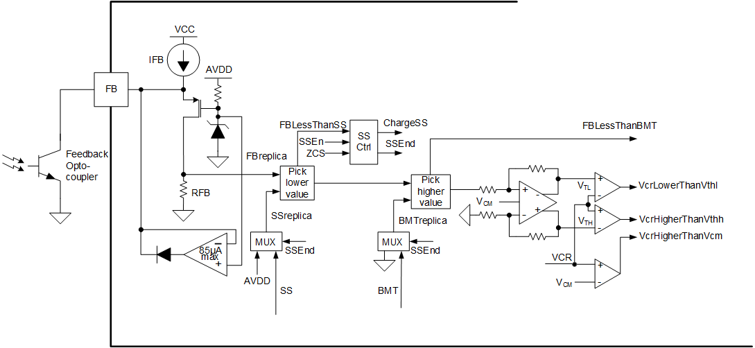
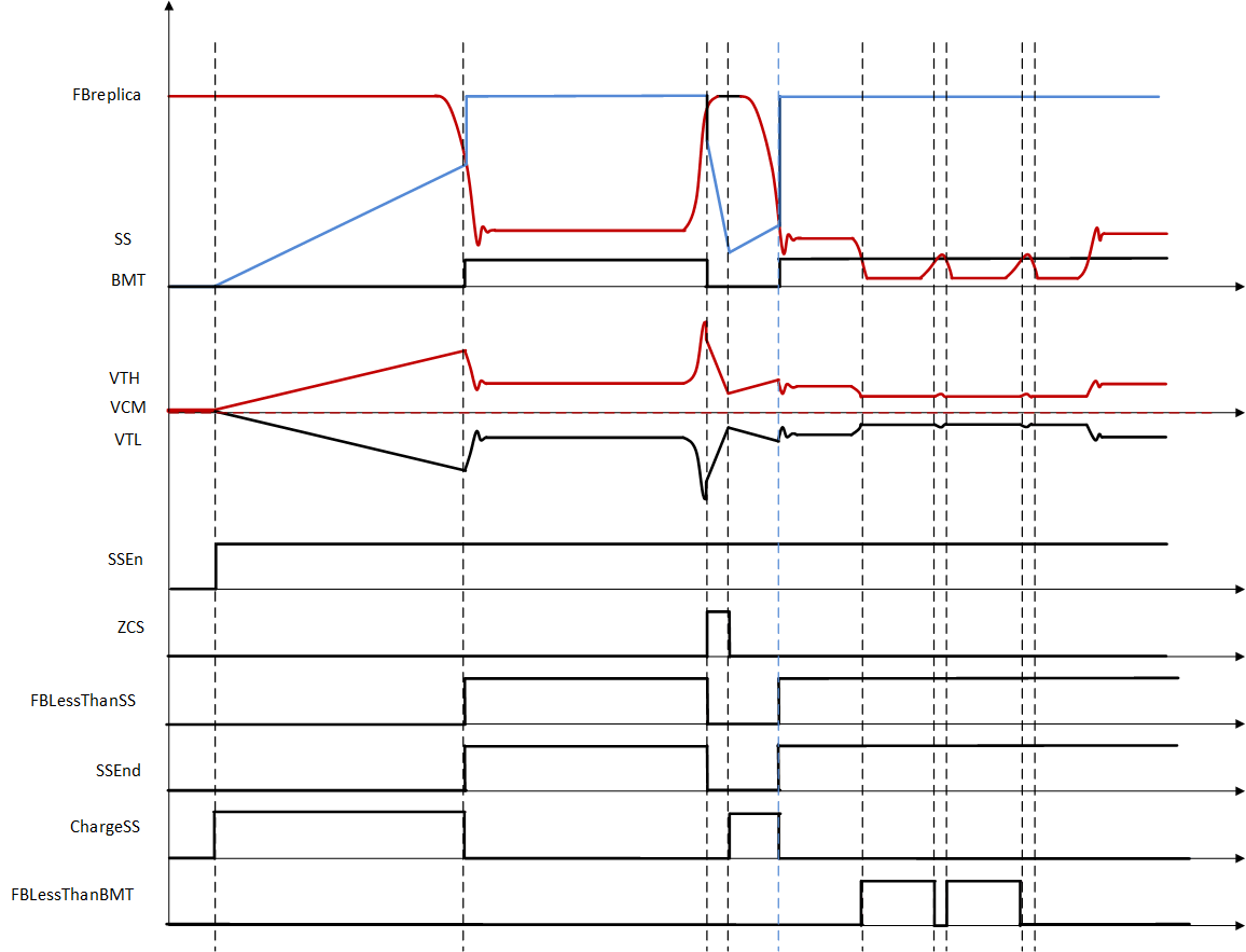
Control of the output voltage is provided by a voltage regulator circuit located on the secondary side of the isolation barrier. The demand signal from the secondary regulator circuit is transferred across the isolation barrier using an optocoupler and is fed into the FB pin on UCC25640x. This section discusses the whole feedback chain. Figure 7-3 shows the block diagram of the FB chain, and Figure 7-4 shows the typical timing diagram with a normal soft start followed by a ZCS event, and load step into burst mode, and then exiting burst mode.
The feedback chain has the following functions:
- Optocoupler feedback signal input and bias
- FB voltage clamp
- Soft start function selection by a "pick lower value" block
- Burst mode selection by a "pick higher value" block
- Convert single ended feedback demand into two thresholds VTH and VTL; and VCR comparison with the thresholds and the common mode voltage VCM
 Figure 7-3 Feedback Chain Block Diagram
 Figure 7-4 Feedback Chain Timing Diagram