ZHCSJY8E june 2019 – february 2021 UCC256402 , UCC256403 , UCC256404
PRODUCTION DATA
- 1 特性
- 2 应用
- 3 说明
- 4 Revision History
- 5 Pin Configuration and Functions
- 6 Specifications
-
7 Detailed Description
- 7.1 Overview
- 7.2 Functional Block Diagram
- 7.3 Feature Description
- 7.4
Device Functional Modes
- 7.4.1 High Voltage Start-Up
- 7.4.2 X-Capacitor Discharge
- 7.4.3 Burst Mode Control
- 7.4.4
System State Machine
-
Application and Implementation
- 8.1 Application Information
- 8.2
Typical Application
- 8.2.1 Design Requirements
- 8.2.2
Detailed Design Procedure
- 8.2.2.1 LLC Power Stage Requirements
- 8.2.2.2 LLC Gain Range
- 8.2.2.3 Select Ln and Qe
- 8.2.2.4 Determine Equivalent Load Resistance
- 8.2.2.5 Determine Component Parameters for LLC Resonant Circuit
- 8.2.2.6 LLC Primary-Side Currents
- 8.2.2.7 LLC Secondary-Side Currents
- 8.2.2.8 LLC Transformer
- 8.2.2.9 LLC Resonant Inductor
- 8.2.2.10 LLC Resonant Capacitor
- 8.2.2.11 LLC Primary-Side MOSFETs
- 8.2.2.12 LLC Rectifier Diodes
- 8.2.2.13 LLC Output Capacitors
- 8.2.2.14 HV Pin Series Resistors
- 8.2.2.15 BLK Pin Voltage Divider
- 8.2.2.16 ISNS Pin Differentiator
- 8.2.2.17 VCR Pin Capacitor Divider
- 8.2.2.18 BW Pin Voltage Divider
- 8.2.2.19 Soft Start and Burst Mode Programming
- 8.2.3 Application Curves
-
Application and Implementation
- 8 Power Supply Recommendations
- 9 Layout
- 10Device and Documentation Support
7.4.3.1 Soft-Start and Burst-Mode Threshold
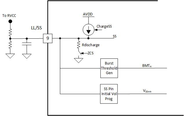
The soft-start programming and burst mode threshold programming are multiplexed on the pin LL/SS. In addition, when ZCS region operation happens, this pin is pulled down to ground through a diode to increase the switching frequency. The pin block diagram is shown in Figure 7-19.
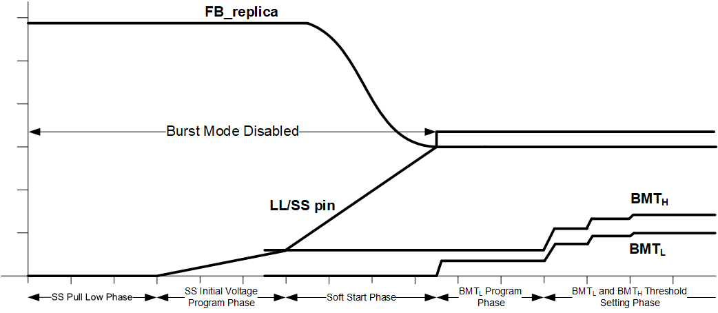
Figure 7-20 shows the timing diagram of the LL/SS pin programming. It includes 5 phases:
- SS pull low phase - LL/SS pin is internally pulled low with a typical 1.2 kΩ resistor to ground.
- SS initial voltage program phase - The internal pull low is released. As shown in Figure 7-19, LL/SS pin is typically connected with a resistor divider from RVCC and a capacitor to ground. When the internal pull low circuit is released, LL/SS pin voltage can be charged up depending on the external resistor and capacitor. This phase ends when charge boot stage is completed and it has a fixed time of tSSInitVolPrgm.
- Soft start phase - An internal constant current source charges the soft start capacitor right after the charge boot stage, and ends when FBreplica becomes lower than the LL/SS pin voltage. During this phase, LL/SS pin voltage is used as the control effort Vcomp. The slow ramp up of LL/SS pin helps the LLC operate at a higher switching frequency when the output voltage is not established yet during startup. This can avoid the large inrush current during startup.
- BMTL settling phase - When soft start phase is completed, LL/SS pin is used for burst mode threshold programming. As described in Section 7.4.3, two burst mode thresholds are used. During this phase, BMTH is fixed at either 0.6V (1.2 V if BW option 7 is selected). BMTL is also fixed which is determined by the programmed ratio of BMTL/BMTH. The typical duration of this phase is 600 us.
- BMTL and BMTH programming/setting phase - LL/SS pin is buffered at 3.5 V during this phase. Depending on the resistors connected to the pin, LL/SS pin could either sink or source current. If LL/SS pin sinks current, the current will be internally mirrored to flow through RLL, and the voltage on RFB is the programmed voltage of BMTH. If LL/SS pin sources current, the programmed voltage of BMTH is set to minimal. If the programmed voltage of BMTH is different from the initial voltage, BMTH ramps to the target value at a refresh frequency of every 200 us. The slow refresh frequency makes sure that BMTH does not change due to the noise on LL/SS pin. BMTL follows the change of BMTH based on the programmed ratio of BMTL/BMTH.
The programmability of the SS initial voltage provides a freedom to limit the maximum switching frequency during startup. This helps to prevent hard switching due to excessively high switching frequency. For applications that require very high switching frequency during startup, an option is also provided to disable the SS initial voltage programming through BW pin, as described in Section 7.4.3.2. If this option is selected, LL/SS pin continues pull low with the internal 1.2 kΩ resistor during the SS initial voltage program phase.
 Figure 7-19 LL/SS Block Diagram
 Figure 7-20 Timing Diagram of LL/SS Pin Programming