ZHCSNM5C november 2020 – august 2023 UCC25800-Q1
PRODUCTION DATA
- 1
- 1 特性
- 2 应用
- 3 说明
- 4 Revision History
- 5 Device Comparison Table
- 6 Pin Configuration and Functions
- 7 Specifications
- 8 Detailed Description
- 9 Application and Implementation
- 10Power Supply Recommendations
- 11Layout
- 12Device and Documentation Support
- 13Mechanical, Packaging, and Orderable Information
8.3.3 External Synchronization
An external signal connected to the SYNC pin synchronizes the switching frequency of the UCC25800-Q1 transformer driver.
In the external synchronization mode, the switching frequency of the SW pin is half of the SYNC pin signal frequency. Given that, to ensure the output voltage remains within the normal operation range, the half of the frequency of external synchronization signal needs to be between 15% and 30% (nominal) above the programmed switching frequency with a tolerance of 5% or less, as described in Equation 2. A minimum high and low pulse width of 150 ns is required. The SYNC pin logic is compatible with TTL and CMOS levels for the design simplicity. It is recommended to use 50% duty cycle signal.
where
- fSW is the RT pin programmed SW-pin switching frequency
- fSYNC is the SYNC pin signal frequency
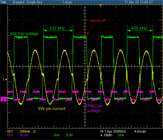
The transformer driver ignores the external synchronization signal during the 1.5-ms soft-start time. The switching frequency during the soft-start time is based on the RT pin voltage as described in Section 8.3.2. After the soft-start period ends, if an external synchronization signal is present and its frequency and pulse width are within the specified range, the switch node is driven by the SYNC pin signal. The transformer driver also integrates a hand-off algorithm so that when the switching frequency transitions from internal oscillator to the external synchronization signal, the disturbance is minimal and transformer saturation is avoided.
The hand-off algorithm first confirms that the external synchronization signal is within the range. If the frequency is not within the acceptable range, the hand-off doesn't happen. If the frequency is within the acceptable range, the hand-off algorithm begins to search for the optimal transition point and locks the switching frequency with the external SYNC signal. After the frequency is locked, the hand-off algorithm stops monitoring the SYNC pin frequency. It is important to ensure external synchronization source has a stable frequency. There is an internal watchdog timer to prevent the external frequency from falling below the set frequency (the watchdog time does not monitor if the SYNC pin frequency goes above the range). If the SYNC pin frequency drops below the set frequency, the transformer driver loses synchronization and the converter operates with the set frequency determined by RT pin voltage.
The Figure 8-5 shows an oscilloscope screen capture for the controller transition from internal oscillator to the external synchronization signal. The smooth transition can be observed and the SW pin current sees minimal disturbance.
 Figure 8-5 Transition from internal oscillator to
external synchronization
Figure 8-5 Transition from internal oscillator to
external synchronizationThe internal MOSFET gate drives are toggled on each SYNC pin voltage rising edge, so the switch-node frequency is equal to half of the SYNC pin signal frequency, as shown in Figure 8-6. Due to the internal filter delays, the SW pin switching edge is not aligned with the SYNC pin switching edge. There is a delay of approximately 150 ns.
 Figure 8-6 External SYNC signal drives switching
frequency